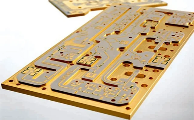
As semiconductor technology advances into microwave and mmWave frequency bands, accurate and repeatable testing becomes increasingly challenging. Microwave IC Test PCBs are specifically engineered to support high-frequency signal integrity, low insertion loss, and precise mechanical alignment, making them essential for validating microwave ICs used in 5G, radar, satellite communication, and high-speed wireless systems.
A professionally designed microwave IC test PCB serves as the critical interface between microwave chips and automated test equipment (ATE), enabling reliable functional, parametric, and performance testing throughout the product lifecycle.
What Is a Microwave IC Test PCB?
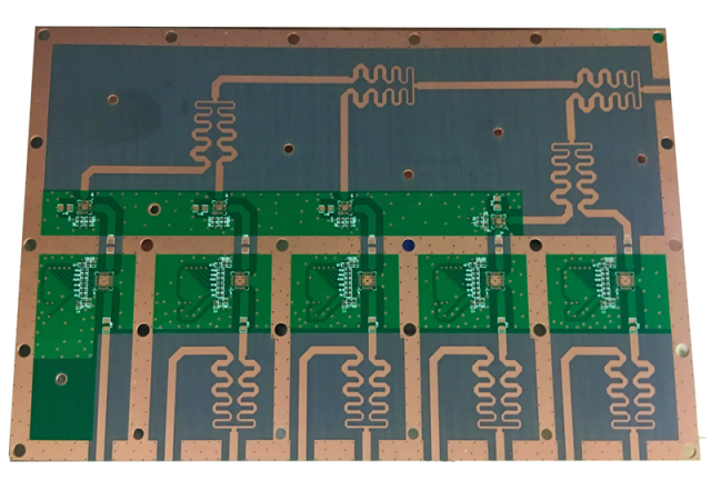
A Microwave IC Test PCB is a high-performance printed circuit board designed for testing microwave and mmWave integrated circuits. It connects the device under test (DUT) to ATE systems, probe cards, or RF test fixtures while preserving signal integrity at extremely high frequencies.
Key functions include:
-
High-frequency signal routing from microwave ICs to test instruments
-
Controlled impedance for GHz and mmWave signals
-
Ultra-low insertion loss and reduced signal reflections
-
Mechanical stability for accurate probe and socket alignment
These PCBs are engineered for precision, repeatability, and reliability in demanding microwave test environments.
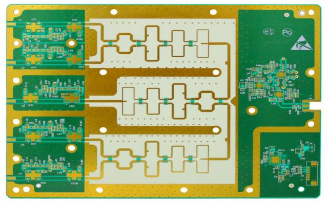
Key Features of Microwave IC Test PCBs
-
Ultra-Low Loss Signal Transmission
Designed to minimize attenuation and distortion at microwave and mmWave frequencies. -
Controlled Impedance Accuracy
Ensures stable RF performance and accurate S-parameter measurements. -
High-Density and High Pin Count Design
Supports advanced microwave ICs with fine-pitch pads and complex I/O layouts. -
Multilayer and HDI Structures
Optimized stackups reduce crosstalk and isolate RF, digital, and power signals. -
Mechanical Precision and Durability
Maintains consistent probe alignment during repeated high-frequency test cycles.
Materials and Stackup Considerations
Material selection is critical for microwave IC test PCB performance:
-
Low-Loss RF Laminates such as Rogers RO4003, RO4350B, Taconic RF-35, and Duroid 5880/6002
-
Hybrid Stackups combining RF materials with high-Tg FR-4 for mixed-signal designs
-
Thermally Stable Materials to prevent warpage during extended microwave testing
-
Optimized copper thickness and surface finishes for stable RF performance
Proper materials and stackup design ensure low dielectric loss, stable impedance, and repeatable microwave measurements.
Applications of Microwave IC Test PCBs
Microwave IC test PCBs are widely used in:
-
Microwave and mmWave IC functional and parametric testing
-
5G and mmWave RF front-end module validation
-
Radar, satellite, and aerospace semiconductor testing
-
Wafer-level microwave probing and package-level testing
-
ATE systems, probe cards, and microwave load boards
These applications demand extreme signal integrity, precision routing, and mechanical stability, all provided by professional microwave IC test PCB solutions.
Choosing a Microwave IC Test PCB Manufacturer
When selecting a microwave IC test PCB supplier, consider:
-
Proven experience in microwave and mmWave PCB manufacturing
-
Expertise in controlled impedance and low-loss RF materials
-
Capability to produce multilayer, HDI, and high-pin-count PCBs
-
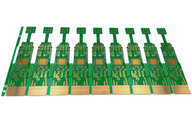
Support for prototype, small-batch, and volume production
-
Robust RF testing, quality control, and engineering support
An experienced manufacturer ensures accurate microwave IC testing, reduced development risk, and faster validation cycles.
Conclusion
Microwave IC Test PCBs are essential for validating high-frequency and mmWave semiconductor devices, offering controlled impedance, ultra-low loss routing, high-density interconnects, and mechanical precision. From 5G and radar to satellite communications, a high-quality microwave IC test PCB enables accurate testing, reliable performance, and efficient transition from R&D to mass production.
