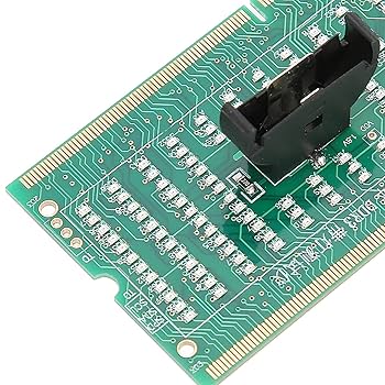
As memory devices continue to evolve toward higher speed, higher density, and lower power consumption, precise testing becomes increasingly critical. A well-designed Memory Test PCB is essential for validating the performance, reliability, and functionality of DRAM, NAND Flash, and other memory ICs throughout development and production stages.
Memory test PCBs provide the electrical interface between memory devices and automated test equipment (ATE), ensuring accurate signal transmission and repeatable test results.
What Is a Memory Test PCB?
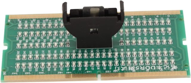
A Memory Test PCB is a specialized printed circuit board used for testing memory ICs under various electrical, timing, and environmental conditions. It supports functional testing, speed binning, reliability validation, and failure analysis of memory chips.
Unlike standard application PCBs, memory test PCBs are optimized for high-speed signaling, tight timing control, and long-term test stability.
Key Requirements for Memory Test PCBs
High-Speed Signal Integrity
Modern memory devices operate at very high data rates. Memory test PCBs must maintain excellent signal integrity with minimal loss, jitter, and crosstalk.
Controlled Impedance Routing
Precise impedance control is critical for accurate timing and signal measurement in DRAM and NAND testing, especially for high-speed interfaces.
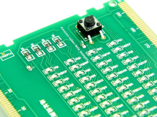
High Pin Count and Dense Routing
Memory ICs often feature a large number of I/O pins, requiring dense routing, fine line fabrication, and reliable interconnect structures.
Electrical Stability and Repeatability
Stable dielectric materials and tight manufacturing tolerances ensure consistent electrical performance across repeated test cycles.
Memory Test PCB Design Considerations
Successful memory test PCB design focuses on:
-
Optimized multilayer stack-up
-
Short and matched signal trace lengths
-
Solid power and ground planes
-
Low-noise power distribution
-
Careful placement of memory sockets and connectors
Design accuracy directly impacts test correlation and measurement reliability.
Materials Used in Memory Test PCBs
Material selection depends on test speed and performance requirements:
-
High-Tg FR-4 for standard memory testing
-
Low-loss laminates for high-speed memory interfaces
-
Hybrid stack-ups for mixed-signal memory test applications
Low dissipation factor and stable dielectric constant are essential for high-frequency memory testing.
Manufacturing Capabilities for Memory Test PCBs
Professional memory test PCB manufacturing includes:
-
Fine line and spacing capability
-
Multilayer and HDI PCB fabrication
-
Blind and buried vias when required
-
Tight impedance and thickness control
-
100% electrical testing and inspection
These processes ensure reliable and repeatable test performance.
Memory Test PCB Assembly Services
Many memory test projects require full PCB assembly, including:
-
Memory IC test sockets
-
High pin count connectors
-
Precision SMT components
-
Mixed SMT and through-hole assembly
Accurate assembly ensures reliable electrical contact and mechanical stability during testing.
Applications of Memory Test PCBs
Memory test PCBs are widely used in:
-
DRAM and NAND Flash testing
-
Memory performance validation
-
ATE-based memory testing systems
-
Reliability and endurance testing
-
Failure analysis and debug
Each application demands high accuracy and consistency.
Prototype and Small Batch Memory Test PCBs
During memory IC development, prototype and small batch memory test PCBs enable rapid validation and test program development. Fast turnaround and engineering support help shorten development cycles and reduce time-to-market.
Small batch production allows design optimization before volume testing.
Why Choose a Specialized Memory Test PCB Manufacturer?
An experienced memory test PCB supplier provides:
-
Deep understanding of memory test requirements
-
Precision fabrication and strict quality control
-
Support for high-speed and high pin count designs
-
Flexible volumes from prototype to production
This expertise ensures memory test PCBs meet the demanding standards of modern semiconductor testing.
Conclusion
Memory Test PCB manufacturing is a critical part of DRAM, NAND, and high-speed memory validation. With optimized design, controlled impedance, and precision manufacturing, memory test PCBs deliver stable signal integrity, accurate measurements, and reliable test performance.
Choosing a professional memory test PCB manufacturer helps ensure consistent results and efficient memory device testing.
