As memory devices continue to evolve toward higher density, higher speed, and lower power consumption, accurate and repeatable testing has become increasingly critical. Memory Test PCBs serve as the core interface between memory chips and automated test equipment (ATE), enabling reliable functional, parametric, and performance testing across the entire memory development and production cycle.
A well-engineered memory test PCB ensures stable signal transmission, precise mechanical alignment, and long-term durability, helping manufacturers improve test accuracy, yield, and overall product reliability.
What Is a Memory Test PCB?
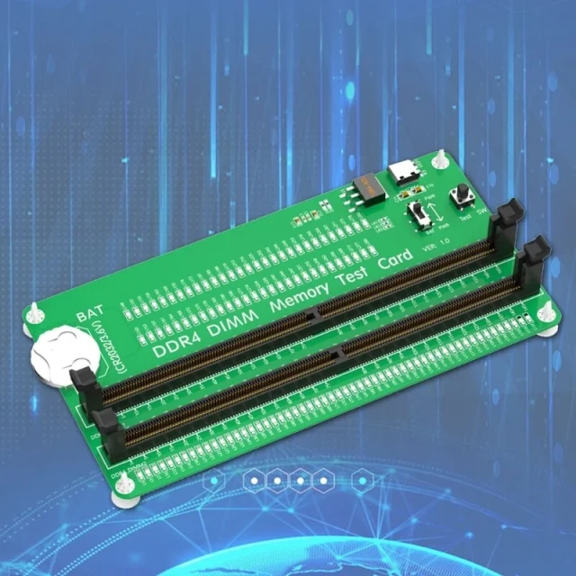
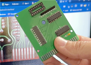
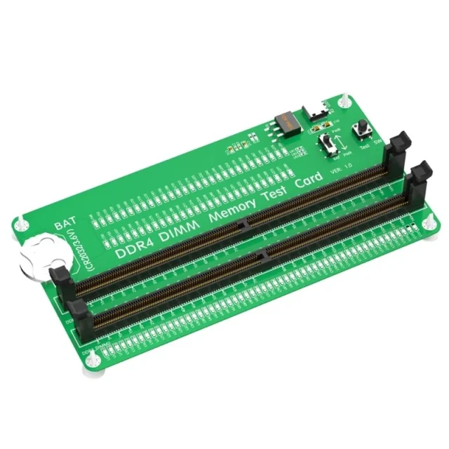
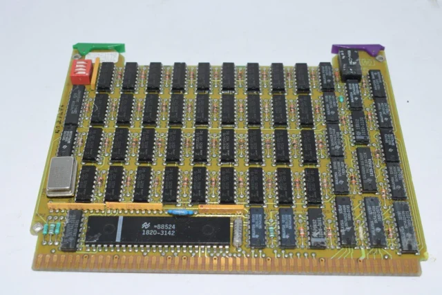
A Memory Test PCB is a specialized printed circuit board designed specifically for testing memory devices such as DRAM, SRAM, Flash, and NAND/NOR memory. It connects the device under test (DUT) to ATE systems through test sockets, load boards, or probe cards.
Key functions include:
-
High-density routing for high-pin-count memory devices
-
Controlled impedance for high-speed data and clock signals
-
Mechanical precision for stable socket or probe alignment
-
Support for repeated test cycles and long-duration testing
Memory test PCBs are engineered for accuracy, repeatability, and reliability in demanding test environments.
Key Features of Memory Test PCBs
-
High-Density and High Pin Count Design
Supports advanced memory packages with hundreds or thousands of I/O connections using fine-line and HDI routing. -
Controlled Impedance and Signal Integrity
Ensures stable transmission of high-speed memory signals, minimizing crosstalk, jitter, and signal loss. -
Multilayer and HDI Stackups
Separates signal, power, and ground planes to reduce noise and improve electrical performance. -
Mechanical Stability and Precision
Maintains accurate socket or probe positioning during repeated insertion and test cycles. -
Thermal and Electrical Reliability
Designed to withstand burn-in testing, high-current operation, and long-term memory stress tests.
Materials and Stackup Considerations
Selecting the right materials is essential for memory test PCB performance:
-
High-Tg FR-4 for standard memory testing applications
-
Low-loss laminates for high-speed DDR and advanced memory technologies
-
Hybrid stackups combining FR-4 with specialized materials for optimized performance
-
Thermally stable cores to prevent warpage during repeated thermal cycling
Proper materials ensure signal integrity, dimensional stability, and reliable long-term performance.
Applications of Memory Test PCBs
Memory test PCBs are widely used in:
-
DRAM, SRAM, and Flash memory functional testing
-
High-speed DDR and advanced memory validation
-
Wafer-level and package-level memory testing
-
ATE load boards and test sockets
-
Prototype verification and mass production testing
These applications demand high-speed signal integrity, mechanical precision, and repeatable performance, all enabled by professional memory test PCB solutions.
Choosing a Memory Test PCB Manufacturer
When selecting a memory test PCB supplier, consider:
-
Experience in semiconductor and memory test PCB manufacturing
-
Capability for multilayer, HDI, and high-pin-count designs
-
Expertise in controlled impedance and high-speed memory interfaces
-
Support for prototype, small-batch, and volume production
-
Strong quality control and electrical testing capabilities
An experienced manufacturer ensures accurate testing, reduced failure rates, and faster development cycles.
Conclusion
Memory Test PCBs are a critical component of semiconductor testing, providing high-density routing, controlled impedance, mechanical stability, and thermal reliability. From DRAM and SRAM to Flash memory, a high-quality memory test PCB enables accurate validation, efficient testing, and a smooth transition from development to mass production.
