Engineering Stable High-Frequency Performance Through KKPCB’s RF-35 Process Integration
From 5G Front-End Design to RF Manufacturing Stability
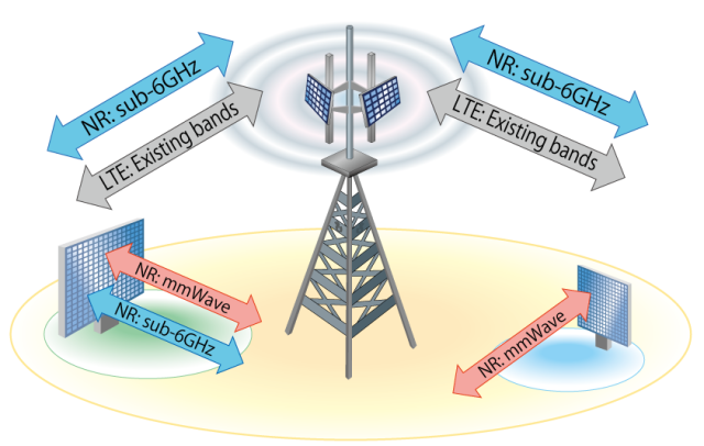
As 5G base station modules scale into the 24–39 GHz spectrum, RF filters and directional couplers become critical for maintaining signal purity, low insertion loss, and high power handling.
Each decibel of loss in a filter path translates directly to reduced coverage, distorted beam patterns, and lower system efficiency.
Taconic RF-35 laminate, with a Dk = 3.5 ± 0.05 and Df = 0.0018 @ 10 GHz, offers a balance between low dielectric loss and mechanical stability—making it ideal for antenna feed networks, filters, and couplers in 5G macro and small-cell radios.
However, achieving consistent high-frequency performance in mass production requires careful control of etching precision, dielectric uniformity, and plating consistency—areas where KKPCB’s RF process control delivers measurable reliability and performance stability.
RF Design Considerations for Low-Loss Filters and Couplers
At mmWave frequencies, even minor material or process deviations can degrade performance:
| Design Parameter | Challenge | Performance Impact |
|---|---|---|
| Dielectric Uniformity | ±0.05 Dk variation | Shifts center frequency and filter Q-factor |
| Conductor Roughness | Excessive copper Ra | Insertion-loss increase > 0.1 dB/inch |
| Line Width Tolerance | ±15 µm etch variation | Impedance mismatch > ±5 Ω |
| Lamination Pressure | Uneven resin flow | Phase shift, coupling imbalance |
KKPCB integrates simulation-driven stackup design and inline impedance verification to ensure that each RF-35 board maintains target S-parameters and dimensional tolerance through production.
KKPCB’s RF-35 Process Control Framework
1.Controlled Dielectric and Lamination Stability
-
Pre-bake RF-35 cores (120 °C / 4 h) to eliminate residual moisture
-
Vacuum lamination @ 180 °C / 200 psi / 60 min for void-free bonding
-
Maintain dielectric thickness tolerance ± 8 µm for consistent impedance
2. Copper Surface and Etching Precision
-
Use rolled copper (Ra < 1.0 µm) to minimize conductor-loss
-
±10 µm etching precision via laser-aligned imaging
-
Post-etch impedance tuning validated with inline TDR measurement
3. Inline RF Verification
-
S-parameter verification (S11/S21) up to 40 GHz per IPC-TM-650
-
Insertion-loss uniformity < 0.08 dB/inch across production lots
-
VNA traceability to NIST standards for calibration consistency
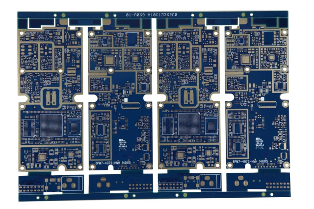
RF-35 PCB
Case Study — 28 GHz Bandpass Filter for 5G Macro Radio
Client: Asian OEM of 5G macro RRUs
Goal: Design a compact, low-loss bandpass filter with ±5 Ω impedance consistency and < 0.3 dB insertion loss @ 28 GHz.
-
Material: RF-35 (0.254 mm) cores + low-flow prepreg
-
Stackup: 4-layer hybrid with FR-4 mechanical support
-
Simulation: 3D EM coupling model tuned to 28 GHz ± 0.25 GHz
-
Process: Controlled copper roughness (Ra < 0.8 µm) and balanced press layup
| Parameter | Target | Achieved |
|---|---|---|
| Insertion Loss @ 28 GHz | < 0.3 dB | 0.27 dB |
| Return Loss | > 20 dB | 21.8 dB |
| Phase Balance | ± 1.2° | ± 0.9° |
| Production Yield | > 96 % | 98.7 % |
Result:
The customer’s 5G radio module improved EIRP by 7 %, while maintaining temperature-stable performance from –40 °C to +125 °C after 1000 thermal cycles.
Extended Application — Directional Coupler for Massive-MIMO Calibration
RF-35’s low-Df substrate enables stable coupling coefficients in 28 GHz MIMO array calibration networks.
KKPCB used dual-line hybrid couplers with ± 0.5 dB coupling tolerance and ± 0.8° phase difference, ensuring accurate power feedback for phased-array beam alignment.
Long-Term Reliability Testing
| Test Type | Condition | Result |
|---|---|---|
| Thermal Cycling | –55 °C ↔ +150 °C / 1000 cycles | No delamination / impedance shift < 3 % |
| Humidity Exposure | 85 °C / 85 % RH / 1000 h | Df drift < 0.0001 |
| Power Load | Continuous RF load 10 W / 3 h | Surface temp rise < 10 °C |
Engineering Insights
RF-35 bridges the performance gap between low-cost FR-4 and premium PTFE materials, enabling scalable, high-frequency PCBs with predictable RF behavior.
Through controlled lamination profiles, micro-etch accuracy, and inline impedance validation, KKPCB transforms RF-35’s material advantages into production-grade stability suitable for 5G filter and coupler manufacturing.
KKPCB’s Quality & Traceability Framework
-
Material lot Dk/Df measurement (≤ ± 0.02 tolerance)
-
3D stackup simulation for CTE balance in hybrid designs
-
Inline VNA verification to 40 GHz
-
Accelerated aging and thermal reliability testing per IPC-TM-650
-
Statistical process control (SPC) for etching and plating uniformity
Conclusion — Turning RF-35 Design into Reliable 5G Performance
RF-35 PCBs enable low-loss RF filter and coupler designs that combine electrical precision with mechanical reliability.
KKPCB’s manufacturing discipline ensures consistent impedance, stable loss characteristics, and traceable performance validation—meeting the rigorous requirements of 5G base station manufacturers.
KKPCB serves as a trusted engineering partner for RF module OEMs seeking repeatable performance from prototype through mass production.
