In semiconductor mass production, test efficiency and accuracy directly impact yield and cost. The Load Board PCB serves as the critical interface between automated test equipment (ATE) and packaged semiconductor devices, enabling stable, repeatable, and high-speed electrical testing.
A professionally engineered load board PCB ensures consistent test results throughout high-volume production.
What Is a Load Board PCB?
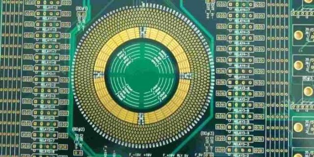
A Load Board PCB is a specialized test board used in semiconductor production testing to:
-
Connect packaged devices to ATE systems
-
Route large numbers of test signals
-
Support sockets, connectors, and mechanical fixtures
Load boards are optimized for durability and repeatability under continuous test cycles.
Why Load Board PCBs Are Essential in Production Testing
Production testing environments demand:
-
High pin count signal routing
-
Stable impedance across all channels
-
Mechanical robustness for repeated insertions
Load board PCBs provide the electrical and mechanical foundation required for reliable high-throughput testing.
Signal Integrity Challenges in Load Board PCBs
As device speeds increase, signal integrity becomes critical. Load board PCBs are designed to:
-
Maintain controlled impedance
-
Minimize crosstalk and signal skew
-
Reduce parasitic effects from vias and connectors
Good signal integrity ensures accurate pass/fail decisions.
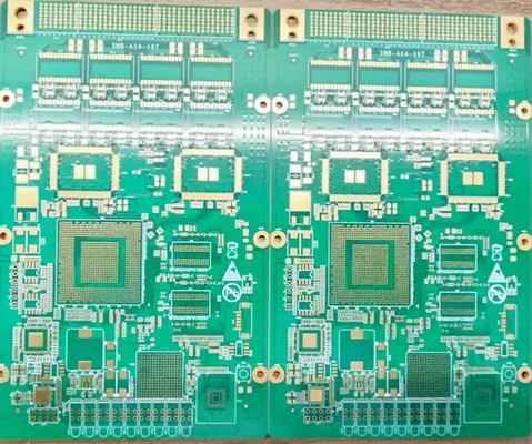
High Pin Count Routing and Stackup Design
Modern load boards often handle hundreds or thousands of signals. Key design features include:
-
Multilayer stackups with dedicated reference planes
-
Fine-line routing for dense breakout
-
Optimized layer assignments for high-speed signals
Advanced stackups improve routing efficiency and electrical performance.
Power Integrity and Grounding Strategy
Load board PCBs must deliver stable power during dynamic testing. Typical solutions include:
-
Solid power and ground planes
-
Low-inductance decoupling capacitor placement
-
Controlled current return paths
Stable power delivery prevents false test failures.
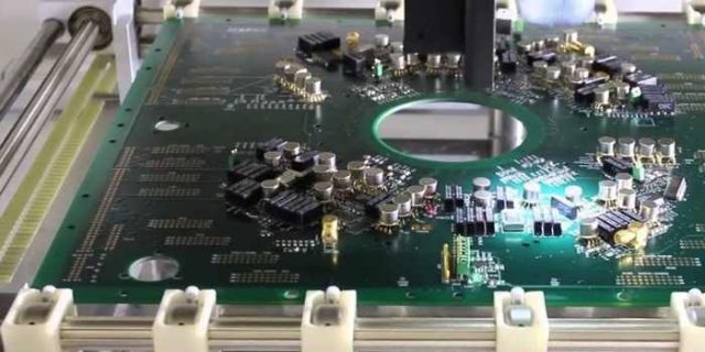
Mechanical Strength and Socket Support
Load boards experience significant mechanical stress. Designs focus on:
-
Reinforced mounting areas for test sockets
-
Controlled board thickness and rigidity
-
Resistance to warpage over long test cycles
Mechanical stability ensures consistent contact quality.
Material Selection for Load Board PCBs
Depending on frequency and test conditions, materials may include:
-
High-Tg FR-4 for structural durability
-
Low-loss laminates for high-speed interfaces
-
Hybrid stackups for performance-cost balance
Material stability supports consistent electrical behavior.
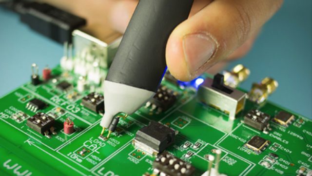
Manufacturing Precision and Quality Control
Manufacturing a load board PCB requires:
-
Tight dimensional tolerances
-
Accurate drilling and plating
-
Electrical continuity and impedance testing
Strict quality control ensures repeatable performance across multiple boards.
Typical Applications of Load Board PCBs
Load board PCBs are widely used in:
-
Semiconductor production screening
-
Final test and system-level test
-
Burn-in and reliability testing
-
High-speed digital and mixed-signal device testing
Each application demands high reliability and consistency.
Choosing a Load Board PCB Manufacturer
When selecting a load board PCB supplier, consider:
-
Experience with semiconductor test boards
-
Capability for high pin count and multilayer designs
-
Controlled impedance expertise
-
Support from prototype to volume production
An experienced manufacturer reduces downtime and test risk.
Conclusion
The Load Board PCB is a mission-critical component in semiconductor production testing. Through optimized signal routing, stable power delivery, and robust mechanical design, load board PCBs enable accurate, repeatable, and high-throughput testing.
Partnering with a professional load board PCB manufacturer ensures long-term reliability and consistent test performance in demanding production environments.
