What is an IoT IC Test PCB?
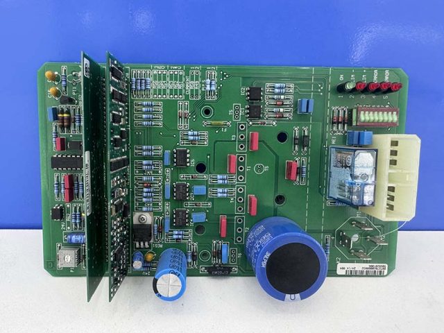
An IoT IC Test PCB is a specialized test board designed for validating, debugging, and verifying integrated circuits used in IoT devices. Unlike standard PCBs, an IoT IC Test PCB is engineered for repeatable testing, accurate measurement, and long-term reliability.
In IoT hardware development, the IoT IC Test PCB acts as a critical interface between the IC and the test system, ensuring that each chip meets performance and quality requirements before deployment or mass production.
Typical use cases of IoT IC Test PCB include:
- IoT chip validation and bring-up
- Functional testing of IoT modules
- Production line testing (FCT / ICT)
- Reliability and burn-in testing
Why IoT IC Test PCB is Essential
With increasing integration in IoT devices, testing complexity is rising. A well-designed IoT IC Test PCB helps:
- Ensure accurate and repeatable test results
- Detect hidden defects early in development
- Improve production yield and reduce failure rates
- Maintain consistent performance across batches
Types of IoT IC Test PCB
1. Evaluation Board (EVB)
An IoT IC Test PCB used during early-stage development to evaluate chip performance and functionality.
2. Functional Test PCB (FCT)
A production-level IoT Test PCB designed to verify whether the circuit performs according to specifications.
3. In-Circuit Test PCB (ICT)
This type of IoT IC Test PCB checks individual components and connections on assembled boards.
4. Burn-in Test PCB
A high-reliability IoT IC Test PCB used to stress-test ICs under elevated temperature and voltage conditions.
Key Design Features of IoT IC Test PCB
1. Optimized Test Point Layout
An IoT IC Test PCB must include clearly defined and accessible test points for accurate probing and fixture integration.
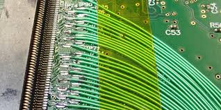
2. High Stability Routing
Stable routing ensures that the IoT IC Test PCB delivers consistent signal behavior during repeated testing cycles.
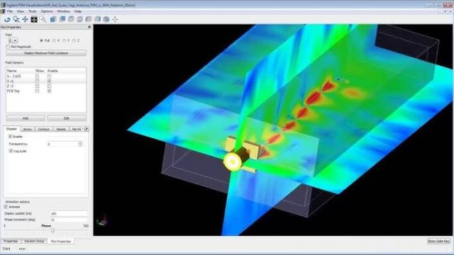
3. Controlled Impedance (for RF IoT devices)
For wireless IoT modules, the IoT IC Test PCB must support controlled impedance to maintain signal integrity.
4. Modular and Replaceable Structure
A modular IoT IC Test PCB design allows easy replacement of ICs or components during testing.
5. Interface Compatibility
The IoT IC Test PCB should be compatible with connectors, sockets, and automated test equipment (ATE).
IoT IC Test PCB and Test Fixture Integration
An IoT IC Test PCB is typically used together with test fixtures and automation systems:
- Pogo pin test fixtures for high-cycle testing
- IC sockets for quick chip replacement
- Automated Test Equipment (ATE) for mass production
Applications of IoT IC Test PCB
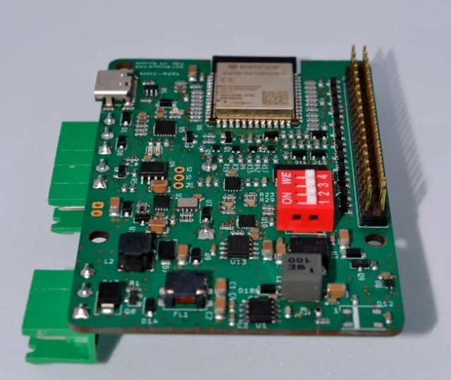
1. Wireless IoT Modules
Testing Wi-Fi, Bluetooth, LoRa, and NB-IoT chips using dedicated IoT IC Test PCB setups.
2. Sensor Devices
Validation of sensor ICs in environmental and industrial IoT applications.
3. Smart Home Electronics
Ensuring functional stability of connected devices through IoT Test PCB systems.
4. Industrial IoT Systems
High-reliability IoT IC Test PCB solutions for harsh operating environments.
5. Automotive IoT
Testing embedded ICs in automotive electronics using robust IoT IC Test PCB designs.
Manufacturing Considerations for IoT IC Test PCB
A high-quality IoT IC Test PCB requires:
- Durable materials for repeated mechanical contact
- High precision fabrication for accurate measurements
- Stable surface finishes for reliable probing
- Consistent production quality across batches
Common Challenges inIoT IC Test PCB
- Contact instability during repeated testing
- Signal inaccuracies due to poor layout
- Wear and degradation over time
- Misalignment with test fixtures
These challenges highlight the importance of experienced IoT IC Test PCB design and manufacturing.
When Do You Need an IoT IC Test PCB?
You should use an IoT IC Test PCB when:
- Developing or validating IoT ICs
- Setting up production testing processes
- Performing reliability or burn-in testing
- Debugging IoT hardware issues
Conclusion
The IoT IC Test PCB is a critical tool in modern IoT hardware development and production. By enabling accurate, repeatable, and reliable testing, it ensures product quality and reduces risks in mass manufacturing.
A well-designed IoT IC Test PCB not only improves testing efficiency but also plays a key role in ensuring long-term product reliability.
