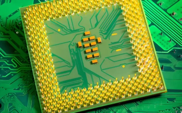
IC Testing PCB: Precision PCB Solutions for Semiconductor Validation
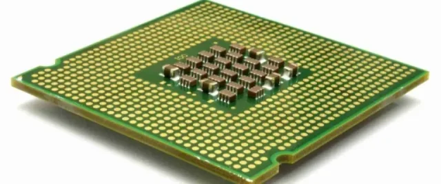
As semiconductor devices grow increasingly complex, accurate testing is more critical than ever. IC Testing PCBs are specialized printed circuit boards designed to interface integrated circuits (ICs) with automated test equipment (ATE), ensuring precise signal transmission, controlled impedance, and reliable mechanical performance during the testing process.
These PCBs are essential for validating device functionality, performance, and yield before mass production.
What Is an IC Testing PCB?
An IC testing PCB serves as the bridge between the device under test (DUT) and the test system. It allows for high-density connections, high-speed signal integrity, and consistent power delivery. Key functions include:
-
Supporting high pin count IC packages
-
Providing stable electrical interfaces for ATE systems
-
Enabling controlled impedance and low-loss signal routing
IC testing PCBs are designed to handle repeated test cycles while maintaining performance consistency.
Key Features of IC Testing PCBs
To ensure accurate semiconductor testing, IC testing PCBs typically incorporate:
-
Controlled Impedance Routing: Reduces signal reflections and preserves high-frequency signal integrity.
-
Multilayer Stackups: Supports complex routing for high pin count ICs and multiple power/ground planes.
-
Mechanical Reliability: Maintains precise alignment with sockets, probe cards, and load boards.
-
High-Speed Signal Support: Ensures minimal signal distortion during fast switching and multi-gigabit testing.
These features ensure that IC testing PCBs deliver repeatable, reliable results across thousands of test cycles.
Material Selection and Stackup Design
Material choice is critical for IC testing PCBs, particularly for high-speed or RF applications. Common selections include:
-
High-Tg FR-4 for standard testing
-
Low-loss laminates for high-frequency or high-speed ICs
-
Optimized hybrid stackups to balance performance and cost
Proper material selection ensures electrical performance and mechanical durability under test conditions.
Applications of IC Testing PCBs
IC testing PCBs are widely applied in:
-
Wafer-level functional and parametric testing
-
IC package validation and characterization
-
Load boards and interface boards for ATE systems
-
High-speed or mixed-signal semiconductor testing
Each application requires precise signal integrity and mechanical stability.
Selecting an IC Testing PCB Manufacturer
When choosing a manufacturer for IC testing PCBs, consider:
-
Experience with high pin count and high-speed IC designs
-
Capability for controlled impedance and multilayer PCB fabrication
-
Support for prototype, small batch, and volume production
-
Strong quality control and electrical testing procedures
A reliable partner ensures that IC testing PCBs meet demanding semiconductor testing requirements.
Conclusion
IC Testing PCBs are a cornerstone of semiconductor validation, providing accurate, repeatable, and reliable electrical connections between ICs and test systems. By combining controlled impedance, multilayer routing, and high mechanical precision, these PCBs enable efficient semiconductor testing from wafer to final product.
Partnering with an experienced IC testing PCB supplier ensures consistent test results, faster development cycles, and higher production yield.
