As integrated circuits become more complex and performance-driven, IC testing PCB plays a critical role in ensuring functionality, reliability, and yield throughout the semiconductor lifecycle. From early-stage IC validation to high-volume production testing, IC testing PCBs provide the electrical interface between the device under test (DUT) and automated test equipment (ATE).
A high-quality IC testing PCB must deliver accurate signal transmission, stable impedance control, and mechanical reliability under repeated test cycles.
What Is an IC Testing PCB?
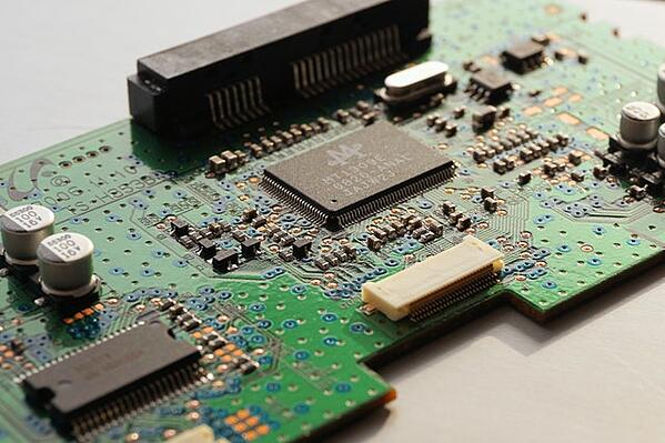
An IC testing PCB is a specialized printed circuit board designed specifically for testing integrated circuits. It is commonly used in semiconductor development, wafer probing, package testing, burn-in, and final test stages.
Unlike standard PCBs, IC testing PCBs prioritize electrical performance, test repeatability, and durability rather than long-term field deployment.
Key Requirements for IC Testing PCBs
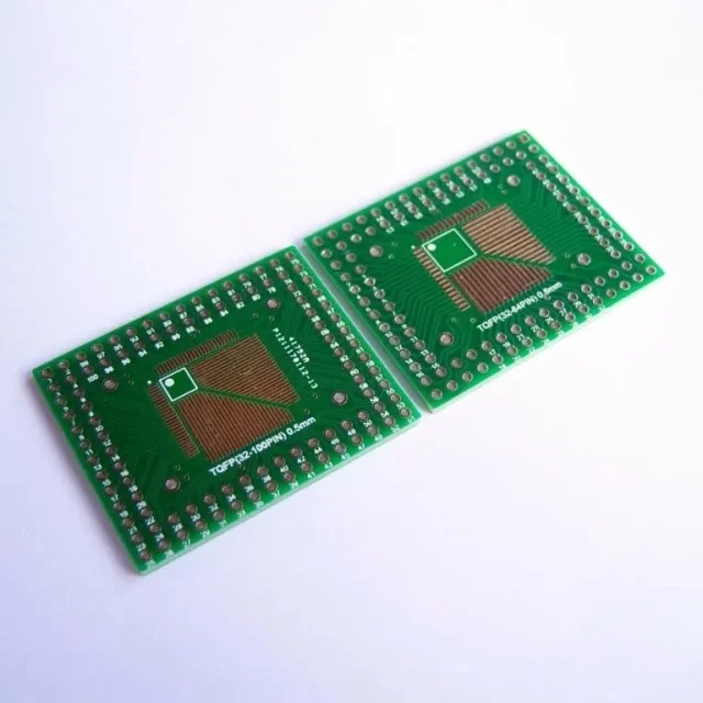
High Pin Count Support
Modern ICs often require hundreds or thousands of test points. IC testing PCBs must support fine-pitch routing, dense fan-out, and high pin count connectors.
Controlled Impedance and Signal Integrity
High-speed IC testing demands strict impedance control, low crosstalk, and minimal signal loss to ensure accurate measurement results.
Stable Electrical Performance
Consistent impedance, low noise, and repeatable electrical behavior are essential for reliable IC testing outcomes.
Mechanical Reliability
IC testing PCBs must withstand frequent insertions, thermal cycling, and long test durations without degradation.
IC Testing PCB Design Considerations
Successful IC testing PCB design typically includes:
-
Optimized multilayer stack-up
-
Controlled impedance routing
-
Short and symmetrical signal paths
-
Power and ground integrity planning
-
Test point and connector layout optimization
Early collaboration between PCB designers and test engineers helps reduce signal distortion and test errors.
Materials Used for IC Testing PCBs
Material selection is critical for IC testing performance. Common materials include:
-
High-Tg FR-4 for standard IC testing
-
Low-loss laminates for high-speed IC testing
-
Hybrid stack-ups for mixed-signal applications
Stable dielectric properties help maintain consistent test conditions.
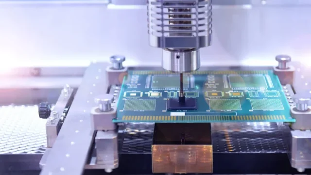
Manufacturing Capabilities for IC Testing PCBs
Advanced IC testing PCB manufacturing requires:
-
Fine line and spacing control
-
Multilayer and HDI capabilities
-
Blind and buried vias when needed
-
Tight thickness and impedance tolerances
-
100% electrical testing
Precision fabrication ensures repeatable performance across test boards.
IC Testing PCB Assembly
Many IC testing applications require PCB assembly services, including:
-
High pin count socket installation
-
Fine-pitch SMT assembly
-
Mixed SMT and through-hole components
-
Connector and probe interface assembly
Careful assembly prevents mechanical stress and ensures test stability.
Applications of IC Testing PCBs
IC testing PCBs are widely used in:
-
Semiconductor R&D validation
-
ATE testing systems
-
Wafer probe testing
-
Package and final test
-
Burn-in and reliability testing
Each application places unique demands on PCB performance and durability.
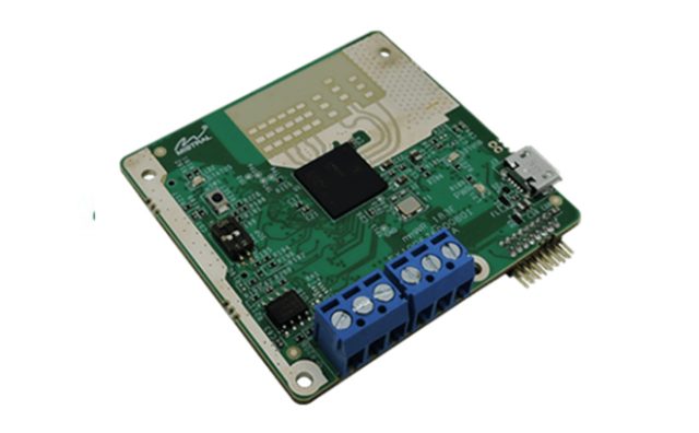
Small Batch and Prototype IC Testing PCBs
IC development often requires small batch or prototype IC testing PCBs for rapid iteration. Fast turnaround and engineering support are essential to keep test programs on schedule.
Prototype IC testing PCBs help identify design issues early and reduce costly rework during mass production.
Why Choose a Professional IC Testing PCB Manufacturer?
A specialized IC testing PCB manufacturer offers:
-
Deep understanding of semiconductor test requirements
-
Precision fabrication and strict quality control
-
Support for custom and non-standard designs
-
Flexible volume from prototype to production
This ensures IC testing PCBs meet demanding performance and reliability standards.
Conclusion
IC testing PCB manufacturing is a critical component of modern semiconductor testing. With precise design, controlled impedance, and high-quality fabrication, IC testing PCBs enable accurate, repeatable, and efficient IC validation.
Partnering with an experienced IC testing PCB supplier ensures stable test results, shorter development cycles, and higher overall test efficiency.
