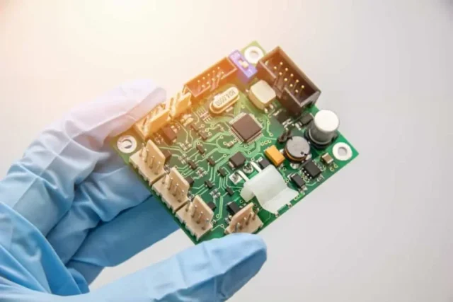
As integrated circuits continue to evolve toward higher speed, higher pin count, and greater functional complexity, IC testing PCB has become a critical component in semiconductor development and mass production. From early silicon validation to final production testing, IC testing PCBs provide the electrical and mechanical interface between the device under test (DUT) and automated test equipment (ATE).
High-quality IC testing PCBs ensure accurate measurements, stable signal integrity, and repeatable test results across demanding semiconductor test environments.
What Is an IC Testing PCB?
An IC Testing PCB is a specialized printed circuit board designed specifically for testing integrated circuits. It is commonly used in:
-
Functional and parametric IC testing
-
Wafer-level and package-level testing
-
Burn-in and reliability validation
-
ATE load boards, probe card interfaces, and test sockets
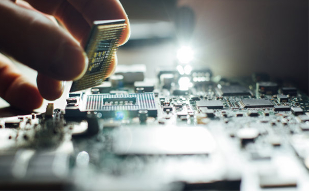
IC testing PCBs must meet far stricter electrical and mechanical requirements than standard application PCBs.
Key Technical Requirements of IC Testing PCB
High Pin Count and Fine-Pitch Routing
Modern ICs often feature hundreds or thousands of I/O pins. IC testing PCBs must support:
-
High pin count layouts
-
Fine-pitch pads and connectors
-
HDI structures with microvias and buried vias
Controlled Impedance and Signal Integrity
Accurate testing depends on clean signal transmission. IC testing PCBs are engineered with:
-
Controlled impedance traces
-
Low crosstalk and minimal signal loss
-
Precise length matching for high-speed signals
Power Integrity and Thermal Stability
Stable power delivery is essential during testing, especially for high-performance ICs. IC testing PCBs incorporate:
-
Low-impedance power planes
-
Optimized decoupling networks
-
Materials with good thermal stability for long test cycles
Materials and Stackup Design for IC Testing PCB
Material selection plays a vital role in IC testing PCB performance. Common options include:
-
High-Tg FR-4 for standard IC testing
-
Low-loss laminates for high-speed or RF ICs
-
Hybrid stackups combining FR-4 and high-frequency materials
-
Thermally stable materials for burn-in and high-current testing
Proper stackup design ensures signal integrity, mechanical reliability, and repeatable test performance.
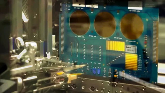
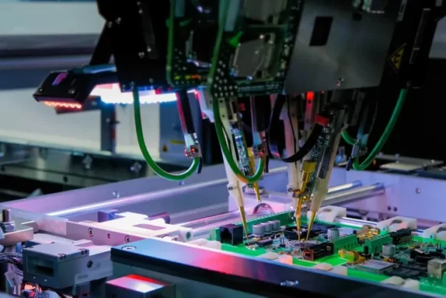
IC Testing PCB Manufacturing Capabilities
Manufacturing IC testing PCBs requires tight process control and advanced capabilities, including:
-
Multilayer PCB fabrication (8–40+ layers)
-
HDI and high-density interconnect technology
-
Tight tolerance drilling and registration
-
Controlled impedance fabrication and verification
Precision manufacturing ensures consistent electrical performance across multiple test boards.
Prototype and Small-Batch IC Testing PCB
IC testing PCBs are often required in prototype or small-batch volumes, especially during new IC development or test program validation.
Advantages of small-batch IC testing PCB production include:
-
Fast engineering validation
-
Flexible design iterations
-
Early detection of layout or signal issues
-
Smooth transition to volume testing
Fast-turn IC testing PCBs help shorten semiconductor development cycles.
Why Choose a Professional IC Testing PCB Manufacturer
Selecting the right IC testing PCB partner directly impacts test accuracy and project timelines. A professional supplier offers:
-
Expertise in semiconductor and ATE applications
-
Strong engineering support for DFM and signal integrity
-
Capability for prototype, small-batch, and volume production
-
Strict quality control and electrical testing
This ensures reliable, repeatable IC testing performance throughout the product lifecycle.
IC Testing PCB Solutions by KKPCB
KKPCB provides high-reliability IC testing PCB solutions for semiconductor and ATE applications. With expertise in high pin count, controlled impedance, HDI, and multilayer PCB manufacturing, KKPCB supports customers from early IC validation to stable production testing.
Whether for load boards, probe card PCBs, or custom IC test interfaces, KKPCB delivers engineering-driven solutions with consistent quality and fast turnaround.
