In the semiconductor industry, accurate testing is critical to ensure IC functionality, yield, and performance. IC Testing PCBs are specialized printed circuit boards that provide a reliable electrical interface between integrated circuits and automated test equipment (ATE), enabling precise measurement and validation across wafers, modules, and final devices.
What Is an IC Testing PCB?
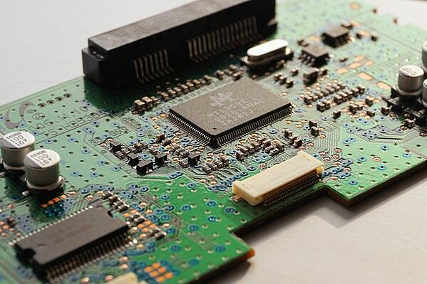
An IC Testing PCB is a custom PCB designed specifically for semiconductor device evaluation. These boards are engineered to meet the demanding requirements of high-speed, high-density ICs, including:
-
Controlled impedance traces for signal fidelity
-
High pin count interconnections for complex IC packages
-
Stable power delivery for accurate testing
IC Testing PCBs are essential for both wafer-level testing and system-level verification.
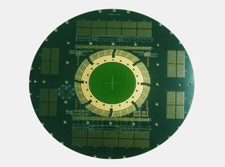
Key Features of IC Testing PCBs
High-quality IC Testing PCBs are distinguished by several critical features:
-
Controlled Impedance Routing: Ensures accurate signal transmission for high-speed ICs.
-
High-Density Layouts: Supports large arrays of IC pins, probe cards, or sockets.
-
Power and Ground Stability: Maintains signal and device integrity during dynamic testing.
-
Robust Mechanical Design: Withstands repeated probe cycles and fixture handling.
These features collectively improve test repeatability and reduce the risk of false failures.
Signal Integrity and High-Speed Testing
Modern ICs often operate at high frequencies and multi-gigabit speeds. IC Testing PCBs are designed to:
-
Minimize crosstalk between adjacent traces
-
Reduce reflections and insertion loss
-
Maintain clean waveforms for ATE measurement
Proper signal integrity design ensures that test results reflect the IC’s true performance.
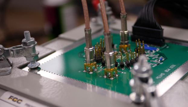
Applications of IC Testing PCBs
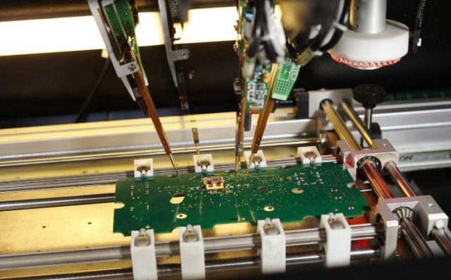
IC Testing PCBs are widely used in:
-
Wafer-level testing and probe card interfaces
-
Load boards for high pin count devices
-
ATE systems for functional, parametric, and reliability testing
-
High-speed IC characterization and validation
Each application benefits from consistent electrical and mechanical performance.
Choosing an IC Testing PCB Manufacturer
When selecting a manufacturer for IC Testing PCBs, important factors include:
-
Experience with high-speed, high-pin-count PCBs
-
Ability to provide controlled impedance and multilayer designs
-
Advanced inspection and testing capabilities
-
Support for prototypes, small batch, and production builds
An experienced partner ensures reliability and minimizes risk during semiconductor testing.
Conclusion
IC Testing PCBs are essential for accurate, reliable semiconductor validation. By combining high-density design, controlled impedance, and robust mechanical features, these boards enable precise IC testing and high yield rates. Partnering with a professional IC Testing PCB manufacturer ensures performance, repeatability, and successful semiconductor test operations from prototype to mass production.
