
Rigid-flex PCB technology combines the advantages of both rigid PCBs and flexible circuits, enabling engineers to achieve compact, lightweight, and highly reliable electronic designs. Compared with traditional rigid boards, rigid-flex PCBs provide greater design freedom by allowing three-dimensional assembly, reducing connector usage, and improving mechanical reliability in applications with limited space.
As electronic products continue moving toward miniaturization, higher integration, and improved reliability, rigid-flex PCB solutions are increasingly used in:
- Medical electronics
- Aerospace and defense systems
- Wearable devices
- Industrial equipment
- Automotive electronics
- High-reliability consumer products
Unlike standard rigid PCBs, flexible and rigid-flex circuits require specialized materials, manufacturing processes, and design strategies to ensure long-term performance.
What Is a Rigid-Flex PCB?
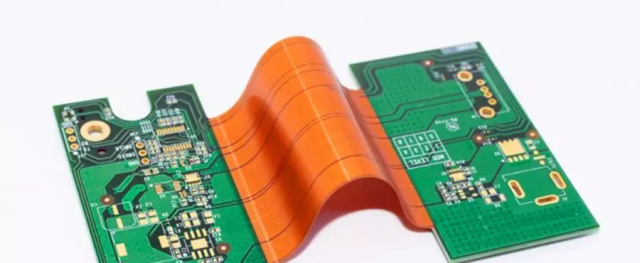
A rigid-flex PCB is a hybrid circuit board that integrates:
- Rigid PCB sections for component mounting and mechanical support
- Flexible PCB sections for bending, folding, and space optimization
A fully flexible PCB uses only flexible materials, while a rigid-flex PCB combines rigid and flexible layers within a single structure.
Compared with conventional PCB solutions, rigid-flex technology provides several advantages:
1. Space Optimization
Rigid-flex PCBs allow electronic assemblies to be folded or arranged in three-dimensional structures, significantly reducing product size.
Benefits include:
- Higher component density
- Reduced wiring space
- Smaller product footprint
- Improved internal assembly flexibility
2. Weight Reduction
By eliminating multiple connectors, cables, and mechanical interfaces, rigid-flex designs can reduce overall system weight.
3. Improved Reliability
Traditional cable connections may introduce:
- Signal loss
- Mechanical failure points
- Assembly complexity
Rigid-flex PCBs integrate interconnections directly into the board structure, improving durability and electrical reliability.
4. Simplified Assembly
A single rigid-flex PCB can replace multiple rigid boards connected by cables or connectors, reducing:
- Assembly steps
- Manufacturing complexity
- Potential connection failures
Key Challenges in Rigid-Flex PCB Manufacturing
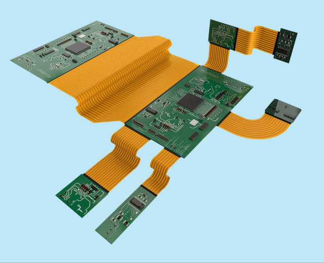
Although rigid-flex PCBs provide significant advantages, their manufacturing process is more complex than traditional rigid PCB production.
Important manufacturing challenges include:
- Thin material handling
- Dimensional stability control
- Coverlay processing
- Precision laser cutting
- Layer alignment
- Controlled impedance design
- Mechanical stress management
A reliable rigid-flex PCB requires strict control throughout the entire manufacturing process.
Rigid-Flex PCB Manufacturing Process
1. Flexible Material Handling
Flexible PCB materials are much thinner and more sensitive than rigid board materials.
Typical flexible materials include:
- Polyimide substrate
- Thin copper foil
- Coverlay layers
- Flexible adhesives
Because flexible materials lack the mechanical reinforcement found in rigid PCBs, improper handling may cause:
- Material deformation
- Wrinkles or folding damage
- Registration errors
- Reduced product reliability
To achieve high manufacturing yield, PCB manufacturers need:
- Specialized handling equipment
- Controlled production environments
- Trained operators
- Proper storage conditions
2. Selective Pad Plating
Selective pad plating is an important process in rigid-flex PCB manufacturing.
Unlike traditional PCB plating, rigid-flex boards require controlled copper deposition only in specific areas.
The process ensures:
- Reliable plated through holes
- Proper pad strength
- Reduced unnecessary copper buildup
- Better flexibility performance
For high-density rigid-flex designs, accurate pad plating control helps maintain:
- Fine-pitch component reliability
- Stable solder joints
- Long-term mechanical durability
3. Polyimide Coverlay Processing
Flexible PCBs typically use polyimide coverlay instead of traditional solder masks.
Coverlay provides:
- Mechanical protection
- Electrical insulation
- Improved bending reliability
The coverlay process requires precise openings for:
- SMT pads
- Through-hole pads
- Connector areas
Common opening methods include:
- Laser cutting
- CNC machining
- Mechanical punching
Laser processing is widely used because it provides:
- High accuracy
- Complex profile capability
- Better alignment control
4. Dimensional Stability Control
One of the biggest challenges in rigid-flex PCB manufacturing is material expansion and contraction.
Flexible materials can change dimensions due to:
- Temperature variation
- Moisture absorption
- Pressure during lamination
These changes may affect:
- Layer registration
- Component alignment
- Circuit accuracy
Manufacturers typically control dimensional variation through:
- Smaller production panels
- Optimized tooling design
- Environmental control
- Advanced registration systems
5. Laser Cutting and Profile Processing
Polyimide materials are suitable for precision laser processing.
Laser cutting enables:
- Complex flexible circuit shapes
- Fine mechanical structures
- High dimensional accuracy
Compared with mechanical routing, laser cutting provides:
- Better edge quality
- Higher design flexibility
- Reduced tooling cost for prototypes
However, manufacturing parameters must be carefully controlled to avoid:
- Carbon residue
- Heat damage
- Material deformation
6. Plasma Desmear and Etching
Rigid-flex PCB structures often include multiple flexible layers.
Because polyimide and flexible adhesives have different chemical characteristics from rigid PCB materials, traditional desmear processes may create reliability risks.
Plasma-based treatment is commonly used because it provides:
- Better process consistency
- Improved hole reliability
- Controlled surface activation
This improves:
- Inner-layer bonding
- Plated hole quality
- Long-term reliability
Material Selection for Rigid-Flex PCBs
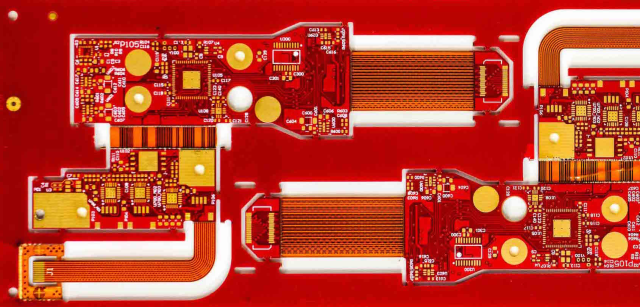
Material selection directly affects PCB performance, flexibility, and reliability.
Polyimide (PI)
Polyimide is the most common flexible PCB material.
Advantages:
- Excellent flexibility
- High temperature resistance
- Good dimensional stability
- Long-term reliability
Applications:
- Wearable electronics
- Medical devices
- Industrial sensors
PEEK (Polyether Ether Ketone)
PEEK materials are used in demanding environments requiring:
- High temperature resistance
- Chemical resistance
- Radiation resistance
Applications:
- Aerospace electronics
- Harsh industrial environments
PTFE Materials
PTFE-based materials are suitable for high-frequency applications.
Advantages:
- Low dielectric loss
- Stable electrical performance
- Excellent thermal characteristics
Applications:
- RF circuits
- High-speed communication systems
Stackup Management in Rigid-Flex PCB Design
Stackup design is one of the most important factors affecting rigid-flex PCB reliability.
A properly designed stackup helps achieve:
- Mechanical flexibility
- Signal integrity
- Controlled impedance
- Reliable lamination
Engineers need to consider:
- Flexible layer thickness
- Copper distribution
- Adhesive thickness
- Bend radius requirements
- Material compatibility
Poor stackup design may result in:
- Delamination
- Mechanical stress concentration
- Impedance variation
- Reduced service life
Flex PCB Bending Requirements
Rigid-flex PCB designs generally involve two types of flexibility:
1. Dynamic Flexing
The PCB repeatedly bends during operation.
Examples:
- Wearable devices
- Folding mechanisms
- Moving electronic assemblies
Design considerations:
- Minimize copper stress
- Avoid sharp bending areas
- Optimize bend radius
2. Static Flex Installation
The PCB only bends during assembly and remains fixed afterward.
Examples:
- Compact electronic modules
- Space-constrained products
These designs usually have lower mechanical requirements compared with dynamic flex applications.
Bend Area Design Guidelines
To improve rigid-flex reliability:
Avoid placing:
- Components
- Vias
- Through holes
- Connectors
near bending areas.
Repeated mechanical stress may cause:
- Copper cracking
- Via failure
- Component damage
Additional design recommendations:
- Use curved trace routing
- Avoid sharp corners
- Maintain proper bend radius
- Strengthen critical areas with coverlay
Trace Routing Optimization for Flexible Areas
Trace design has a major impact on flex PCB durability.
Recommended practices:
1. Route Traces Perpendicular to the Bend Direction
This reduces mechanical stress during bending.
2. Avoid Sharp Trace Corners
Use curved routing to minimize stress concentration.
3. Stagger Double-Sided Traces
For double-layer flex circuits:
- Avoid overlapping traces
- Improve mechanical balance
- Reduce bending stress
4. Maintain Signal Integrity
High-speed rigid-flex designs should consider:
- Controlled impedance
- Ground reference continuity
- Return path optimization
Manufacturing Considerations for High-Reliability Rigid-Flex PCBs
A successful rigid-flex PCB project requires close cooperation between:
PCB Design Team
Focus on:
- Stackup optimization
- Bend analysis
- Signal integrity
- Mechanical constraints
PCB Manufacturer
Focus on:
- Material handling
- Lamination control
- Registration accuracy
- Process reliability
Assembly Partner
Focus on:
- SMT process optimization
- Component placement
- Soldering profile control
Conclusion
Rigid-flex PCB technology provides an effective solution for modern electronic products requiring:
- Compact design
- Lightweight construction
- High reliability
- Mechanical flexibility
- Improved system integration
However, successful rigid-flex PCB manufacturing requires careful control of:
- Material selection
- Stackup design
- Flex area management
- Manufacturing processes
- Signal integrity considerations
By combining advanced PCB fabrication technologies with engineering-driven design optimization, manufacturers can help customers achieve reliable rigid-flex PCB solutions for next-generation electronic applications.
