1. Executive summary
RO3003 (Rogers RO3000 series) is a PTFE-based, ceramic-filled laminate widely adopted where low dielectric loss, stable Dk, and excellent dimensional stability are required. This article explains why RO3003 is often the substrate of choice for automotive radar (e.g., 24 GHz, 77 GHz) and 5G mmWave antenna systems (e.g., 24–40 GHz), then walks through two practical case studies showing stack-ups, critical process controls, measurement targets, and manufacturing considerations. Short, actionable recommendations are provided for engineers and procurement managers evaluating RO3003 solutions.
2. Why RO3003 for radar and mmWave antennas?
Key electrical and mechanical reasons RO3003 is selected:
-
Ultra-low loss (Df ≈ 0.001 @10GHz) — reduces insertion loss on transmission lines and antenna feed networks, improving gain and noise figure.
-
Stable dielectric constant (Dk ≈ 3.00 ±0.04 at 10GHz) — predictable impedance and phase behavior across frequency and temperature.
-
Good dimensional/thermal stability (CTE compatible with copper) — helps maintain registration and impedance after reflow/thermal cycling.
-
Process maturity for PTFE laminates — when produced in experienced facilities, yields can meet automotive and telco reliability standards.
For radar and phased arrays, phase accuracy, low loss and tight impedance control directly influence system performance (beam steering accuracy, sidelobe levels, detection range). For 5G mmWave, low-loss feed networks and predictable element impedance maximize realized antenna gain and minimize insertion loss of filters/dividers.
3. Key electrical & mechanical design parameters to control
When designing RO3003 PCBs for radar / mmWave, prioritize:
-
Impedance tolerance: target ±5% (or tighter for phased arrays).
-
Trace geometry: at mmWave, small changes in substrate thickness or copper roughness alter Zo; model with EM tools.
-
Copper type: rolled copper or reverse-treated copper reduces conductor loss versus very rough foils.
-
Surface finish: ENIG/ENEPIG or immersion silver recommended for RF connectors and soldering — consider tradeoffs in corrosion and skin effect at high frequency.
-
Stack-up control: tight dielectric thickness tolerances (±0.01 mm or better depending on spec).
-
Via technology: laser microvias or carefully controlled thru vias; via stubs and transitions must be minimized for mmWave.
-
Thermal and mechanical control: pre-bake, plasma etch for adhesion, vacuum lamination to avoid voids.
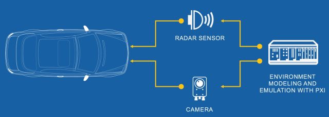
4. Case Study A — 77 GHz Automotive FMCW Radar Module (Typical real-world example)
Objective: High-sensitivity 77 GHz FMCW front-end PCB for long-range radar with integrated antenna and feed network.
Typical electrical goals
-
RF path insertion loss: < 0.8 dB/inch at 77 GHz (aggressive target).
-
Phase variation across array elements: < ±1° (for accurate beamforming).
-
Controlled impedance: 50Ω microstrip and balanced differential nets (100Ω) within ±3–5%.
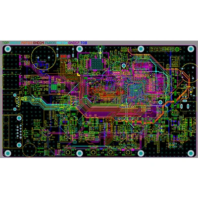
Example stack-up (conceptual)
| Layer | Material | Thickness |
|---|---|---|
| Top | 1 oz Cu (35µm), microstrip traces | — |
| Prepreg | RO3003 core | 0.127 mm (5 mil) |
| Inner plane | Ground | — |
| Core | RO3003 core | 0.127 mm |
| Bottom | 1 oz Cu, ground | — |
Note: Multilayer 6–8 layer designs are common for integrating feed networks and IF/digital circuits separately.
Design & process notes
-
Material thickness: choose thin RO3003 cores (e.g., 5–10 mil) for compact microstrip width while keeping mechanical strength.
-
Copper roughness: use smoother foils; rough foils increase conductor loss at 77 GHz.
-
Via strategy: use plated thru or laser microvias; minimize stub length or apply back-drilling where necessary.
-
Lamination: vacuum lamination at controlled temperatures to avoid voids and maintain registration; pre-treat PTFE with plasma to improve bond.
-
Test & verification: TDR and on-wafer/VNA S-parameter measurements for feed networks; cross-section checks for voids and copper adhesion.
Manufacturing implications
-
Yield risk: without experienced PTFE handling, delamination and registration issues increase scrap.
-
KKPCB role: KKPCB applies dedicated PTFE lamination lines, laser alignment, and microvia processing to meet automotive tolerances and reliability testing (thermal shock, humidity, mechanical vibration).
5. Case Study B — 28/39 GHz 5G Phased-Array Antenna Module
Objective: Compact phased-array submodule for base station or active antenna system (AAS) operating across 24–40 GHz.
Electrical targets
-
Element port match: S11 < −12 dB across band.
-
Feed network insertion loss: as low as possible, target < 1 dB per feed segment.
-
Beamforming phase accuracy: better than ±2° across array.
Example design decisions
-
Substrate selection: RO3003 chosen for low Df to keep feed network loss low and maintain element pattern.
-
Antenna element implementation: patch, slot, or dielectric resonator elements; choice depends on bandwidth & fabrication.
-
Thickness choice: thicker RO3003 cores (e.g., 10–20 mil) can increase bandwidth for patch elements but require careful impedance adjustment.
-
Array layout: feeding microstrip/slot transitions require EM simulation (HFSS, CST) to minimize reflections and mutual coupling.
Stack-up snippet (illustrative)
-
Top: Radiating patch (copper)
-
Dielectric: RO3003 core 0.254 mm (10 mil)
-
Ground/Feed plane: coupled microstrip/slot layer
-
Back: control electronics on FR4 (hybrid stack-up) — use controlled bondply between RO3003 and FR4.
Manufacturing considerations
-
Hybrid lamination: PTFE/FR4 hybrid stack-ups require selection of compatible bondply and controlled lamination schedule to reduce CTE mismatch stress.
-
Panelization & routing: careful panel routing to protect antenna pattern edges and avoid reflections from seam/slot.
-
Qualification: thermal cycling, vibration, and humidity tests per telecom/automotive specs if used in outdoor AAS.
6. Practical EM/Mechanical modeling tips
-
Use 3D full-wave EM solvers for antenna and feed network co-simulation — small geometry changes matter at mmWave.
-
Account for copper roughness models (e.g., Hammerstad or IPC roughness models) in the conductor loss calculations.
-
When simulating impedance, include stack-up tolerances (±thickness) and worst-case Dk variations to ensure robustness.
-
For phase-critical arrays, simulate mutual coupling and verify beam patterns across worst-case manufacturing tolerance scenarios.
7. Testing and validation checklist (recommended)
-
Impedance (TDR): verify target Zo along critical traces.
-
S-parameters (VNA): measure TX/RX feed networks and antenna ports across full band.
-
Insertion loss: measure loss per unit length and per feed stage.
-
Phase/beam testing: validate phased-array beam steering and side lobe levels in anechoic chamber.
-
Reliability tests: thermal cycling, humidity, solderability, and mechanical shock/vibration per application.
8. KKPCB capabilities (subtle, trust-building)
KKPCB provides one-stop RF PCB services that are relevant to the above needs:
-
Material consulting: selection between RO3003, RO4350B, RO4003C based on tradeoffs.
-
DFM & EM support: stack-up proposals, impedance calculation and simulation liaison.
-
PTFE process lines: vacuum lamination, plasma pre-treatment, laser microvia capability.
-
Test & validation: in-house TDR, VNA S-parameter fixtures, cross-section microscopy, and environmental qualification.
We work with customers from prototype through volume production and can tailor lamination schedules and panelization to meet both electrical and cost targets.
9. Practical recommendations (quick checklist)
-
Use RO3003 if: your design requires minimal loss, tight phase control, or long RF feed paths (radar arrays, mmWave beamformers).
-
Use RO4350B if: budget and manufacturability are primary and frequency / performance targets are less extreme.
-
Always: simulate with real copper roughness and stack-up tolerances — then validate with TDR & VNA before committing to volume.
-
Partner with an experienced RF PCB manufacturer to reduce prototyping iterations and avoid yield traps on PTFE laminates.
