A High Layer Count ATE PCB is a critical component in advanced automated test equipment (ATE) used for semiconductor testing, IC validation, and high-speed functional verification. As modern chips continue to increase in complexity, pin count, and data rate, traditional low-layer PCBs can no longer meet routing density and signal integrity requirements.
High layer count ATE PCBs provide the routing capacity, power integrity, and impedance control necessary for accurate and stable test performance.
What Is a High Layer Count ATE PCB?
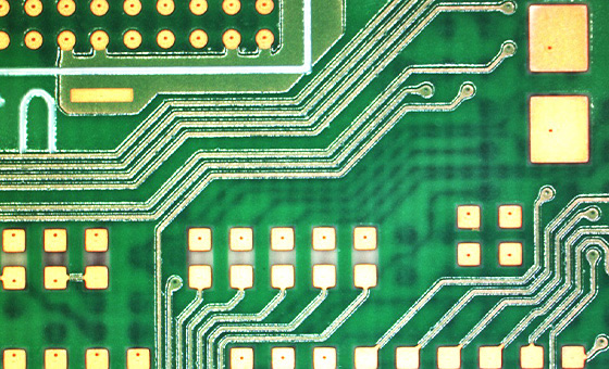
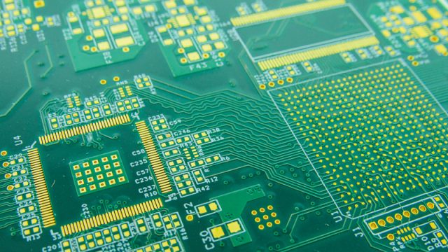
A High Layer Count ATE PCB typically features 16 layers, 20 layers, 24 layers, or more, designed specifically for ATE load boards, interface boards, and test fixtures. These PCBs integrate multiple signal, power, and ground layers to support high pin count devices and complex test architectures.
The multilayer structure enables efficient signal routing while maintaining controlled impedance and minimizing noise and crosstalk.
Why High Layer Count Matters in ATE Applications
Support for High Pin Count Devices
Modern semiconductor devices require thousands of signal connections. High layer count ATE PCBs allow dense fan-out routing from sockets and probe interfaces.
Enhanced Signal Integrity
Dedicated reference planes and optimized layer stacking reduce reflection, skew, and electromagnetic interference.
Improved Power Integrity
Multiple power and ground layers ensure stable voltage delivery for high-speed and mixed-signal testing.
Better Routing Flexibility
Additional layers allow separation of high-speed, analog, and digital signals, improving test accuracy.
Key Design Challenges of High Layer Count ATE PCBs
Controlled Impedance
Precise impedance control across multiple layers is essential for maintaining signal integrity at high frequencies.
High-Speed Signal Management
Differential pair routing, length matching, and via optimization are critical for reliable test signals.
Thermal Management
Dense multilayer designs generate heat, requiring careful thermal design and material selection.
Manufacturing Tolerance
Tight control of layer thickness, alignment, and lamination is necessary for consistency and reliability.
Materials for High Layer Count ATE PCBs
To meet demanding test requirements, high layer count ATE PCBs often use:
-
High-Tg FR-4 materials for thermal stability
-
Low-loss laminates for high-speed signals
-
Mixed-material stack-ups for RF and digital testing
-
Advanced prepregs with controlled dielectric thickness
Material selection is based on test frequency, operating temperature, and mechanical requirements.
Manufacturing Capabilities Required
Producing high layer count ATE PCBs requires advanced fabrication capabilities, including:
-
Multilayer lamination (16–40+ layers)
-
HDI technology with blind and buried vias
-
Laser drilling for fine-pitch routing
-
Controlled impedance fabrication and testing
-
Tight registration and thickness control
These processes ensure reliable electrical performance across all layers.
High Layer Count ATE PCB Assembly
Assembly of high layer count ATE PCBs involves:
-
High pin count socket and connector assembly
-
Fine-pitch component placement
-
X-ray inspection for hidden solder joints
-
Electrical and functional testing
Careful assembly ensures consistent performance during long test cycles.
Applications of High Layer Count ATE PCBs
High layer count ATE PCBs are widely used in:
-
Semiconductor wafer sort systems
-
Final test and burn-in equipment
-
High-speed logic and memory testing
-
RF and mixed-signal ATE platforms
-
Automotive and industrial chip validation
These applications demand extreme reliability and accuracy.
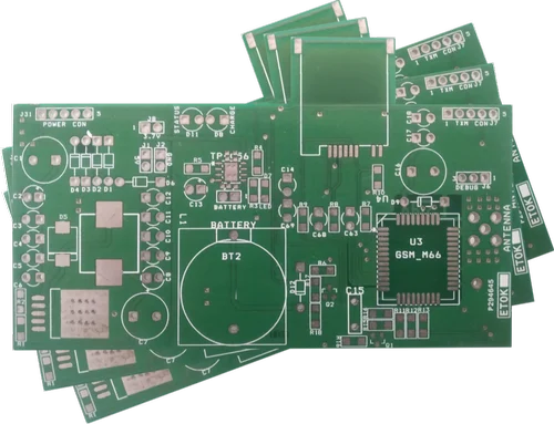
Prototype and Small Batch Production
Most high layer count ATE PCBs begin as prototypes or small batch builds to verify electrical performance and system compatibility. Once validated, designs can be scaled to volume production with stable materials and controlled processes.
Working with an experienced ATE PCB manufacturer reduces development risk and shortens time to market.
Conclusion
A High Layer Count ATE PCB is essential for modern semiconductor test systems that require high pin count support, controlled impedance, and high-speed signal integrity. With advanced materials, precise manufacturing, and expert assembly, these PCBs deliver stable, repeatable test results in demanding environments.
Choosing the right high layer count ATE PCB supplier is key to ensuring long-term performance and reliability.
