As semiconductor devices continue to increase in complexity and pin density, automatic test equipment (ATE) systems require more advanced interconnect solutions. The High Layer Count ATE PCB is specifically engineered to support dense routing, high-speed signal integrity, and stable power delivery in modern semiconductor test environments.
High layer count ATE PCBs play a critical role in ensuring accurate, repeatable, and high-throughput testing.
What Is a High Layer Count ATE PCB?
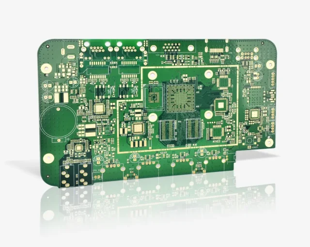
A High Layer Count ATE PCB is a multilayer test circuit board typically featuring 20 layers or more, designed to accommodate complex signal, power, and ground architectures required by advanced ATE systems.
These boards integrate:
-
High-speed digital signals
-
RF and mixed-signal routing
-
Multiple power domains
All within a compact footprint.
Why High Layer Count Is Essential for ATE Systems
ATE platforms must handle thousands of test channels simultaneously. High layer count ATE PCBs enable:
-
Efficient breakout of high pin count devices
-
Dedicated signal, power, and ground layers
-
Reduced crosstalk and electromagnetic interference
This multilayer architecture is essential for test accuracy.
Signal Integrity in High Layer Count ATE PCBs
Maintaining signal integrity across many layers is a major design challenge. High layer count ATE PCBs are optimized through:
-
Controlled impedance routing
-
Symmetrical stackup design
-
Continuous reference planes
These techniques ensure clean signal transmission at high data rates.
Power Integrity and Thermal Management
ATE systems require stable power under dynamic load conditions. High layer count ATE PCBs support:
-
Multiple power planes with low impedance
-
Improved current distribution
-
Enhanced thermal dissipation across layers
This results in reliable long-duration test operation.
Stackup Design and Material Selection
Proper stackup planning is critical for high layer count ATE PCB performance. Key considerations include:
-
Low-loss dielectric materials
-
Balanced layer construction
-
Via structures optimized for high-speed testing
Careful material selection minimizes loss and skew.
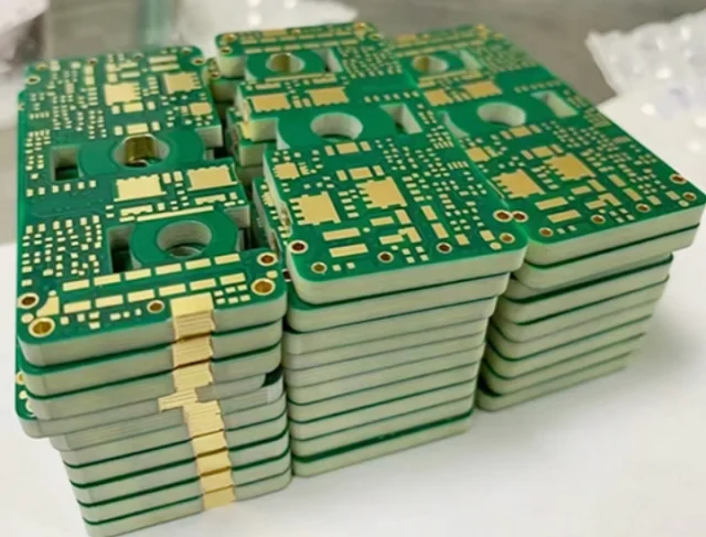
Manufacturing Challenges of High Layer Count ATE PCBs
Producing high layer count ATE PCBs requires advanced manufacturing capability, including:
-
Precise layer-to-layer registration
-
High aspect ratio drilling and plating
-
Strict lamination process control
Quality control is essential to ensure yield and reliability.
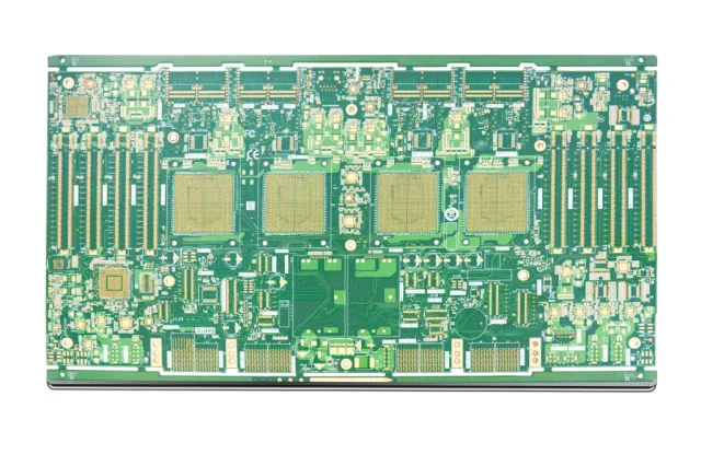
Applications of High Layer Count ATE PCBs
High layer count ATE PCBs are widely used in:
-
Semiconductor final test and wafer sort
-
Load boards and interface boards
-
High pin count device testing
-
Mixed-signal and high-speed IC validation
These applications demand both electrical performance and mechanical stability.
Choosing the Right High Layer Count ATE PCB Manufacturer
When selecting a high layer count ATE PCB supplier, look for:
-
Proven ATE and semiconductor test experience
-
Capability for ultra-high layer counts
-
Controlled impedance and backdrilling expertise
-
Support for prototype, small batch, and volume production
A skilled manufacturer ensures consistent quality across builds.
Conclusion
The High Layer Count ATE PCB is a cornerstone of advanced semiconductor testing, enabling dense routing, reliable power delivery, and superior signal integrity. As test requirements continue to evolve, high layer count PCB technology remains essential for next-generation ATE systems.
Working with an experienced high layer count ATE PCB manufacturer ensures performance, reliability, and scalability from development through production.
