As semiconductor devices continue to scale in pin count, speed, and functionality, test hardware must evolve accordingly. High Layer Count ATE PCBs are specifically engineered to meet the electrical and structural demands of modern automatic test equipment (ATE), supporting dense routing, multiple power domains, and high-speed signal integrity.
These advanced multilayer PCBs form the backbone of reliable and repeatable semiconductor testing.
What Is a High Layer Count ATE PCB?
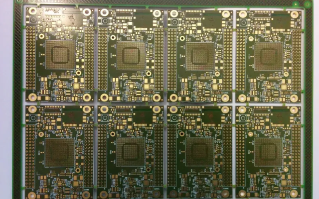
A High Layer Count ATE PCB is a specialized multilayer printed circuit board—often exceeding 20, 30, or even 40 layers—designed for semiconductor test systems. These boards integrate:
-
High-speed digital and mixed-signal routing
-
Multiple power and ground planes
-
High pin count device interfaces
All within a tightly controlled electrical environment.
Why ATE Systems Require High Layer Count ATE PCBs?
Modern ATE platforms test thousands of signals simultaneously. High layer count ATE PCBs make this possible by:
-
Separating signal, power, and ground layers for noise control
-
Supporting dense breakout of high pin count ICs
-
Maintaining signal integrity across long test paths
-
Improving routing efficiency without increasing board size
Higher layer counts directly improve test stability and accuracy.
Signal Integrity in High Layer Count ATE PCBs
Signal integrity is a primary design challenge in high layer count ATE PCBs. These boards rely on:
-
Controlled impedance routing
-
Dedicated reference planes
-
Layer symmetry to minimize skew
-
Backdrilling and via optimization
These techniques reduce crosstalk, reflection, and insertion loss at high data rates.
Power Integrity and Thermal Performance
ATE boards must deliver stable power under dynamic load conditions. High layer count ATE PCBs enable:
-
Multiple low-impedance power planes
-
Short return paths for high-current signals
-
Improved heat distribution across layers
This ensures reliable long-duration test operation.
Stackup Planning and Material Selection
Effective stackup design is critical for high layer count ATE PCBs. Typical considerations include:
-
Balanced layer construction
-
Low-loss dielectric materials for high-speed channels
-
Optimized dielectric thickness for impedance control
Proper material and stackup choices improve both electrical and manufacturing performance.
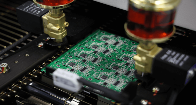
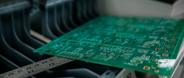
Manufacturing Challenges of High Layer Count ATE PCBs
Fabricating high layer count ATE PCBs requires advanced manufacturing capabilities, such as:
-
Precise layer-to-layer registration
-
High aspect ratio drilling and via plating
-
Multiple lamination cycles with tight process control
-
Strict electrical testing and inspection
Only experienced manufacturers can ensure consistent yield and reliability.
Applications of High Layer Count ATE PCBs
High layer count ATE PCBs are widely used in:
-
Semiconductor final test and wafer sort systems
-
Load boards and interface boards
-
High pin count logic and memory device testing
-
High-speed and mixed-signal ATE platforms
These applications demand maximum electrical performance and stability.
Choosing a High Layer Count ATE PCB Manufacturer
When selecting a High Layer Count ATE PCB manufacturer, look for:
-
Proven experience in semiconductor test PCBs
-
Capability for ultra-high layer counts
-
Controlled impedance and backdrilling expertise
-
Support from prototype to small batch and volume production
A qualified partner ensures long-term test reliability and scalability.
Conclusion
High Layer Count ATE PCBs are essential for supporting the increasing complexity of modern semiconductor testing. By enabling dense routing, stable power delivery, and excellent signal integrity, these multilayer boards ensure accurate and repeatable ATE performance.
Partnering with an experienced High Layer Count ATE PCB supplier is key to achieving reliable test results and efficient test system deployment.
