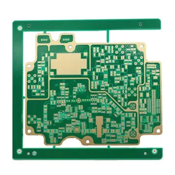
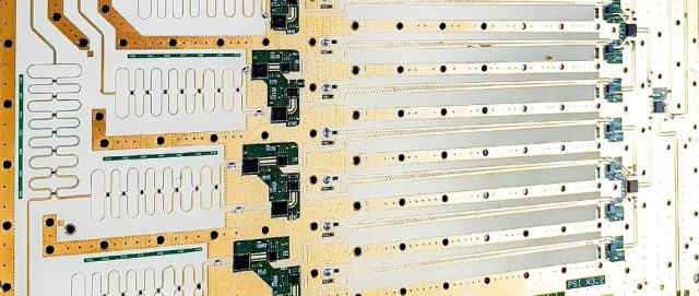
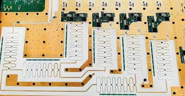
As RF, microwave, and high-speed electronic systems continue to evolve, product complexity and performance requirements are increasing rapidly. Working with a professional high frequency PCB ODM partner allows companies to shorten development cycles, reduce technical risk, and ensure stable high-frequency performance from design to production.
A qualified high frequency PCB ODM provides not only PCB fabrication, but also design optimization, material selection, and manufacturing integration tailored for RF and high-speed applications.
What Is High Frequency PCB ODM?

High frequency PCB ODM (Original Design Manufacturer) refers to a service model where the supplier provides complete or partial PCB design, engineering optimization, and manufacturing for high-frequency and RF applications.
A high frequency PCB ODM typically supports:
-
RF and high-speed PCB layout design
-
Stackup and impedance modeling
-
Material selection for low loss performance
-
PCB fabrication and testing
-
Assembly and validation support
This integrated approach ensures design intent is accurately translated into production.
Why Choose a High Frequency PCB ODM Partner?
Integrated RF Design Expertise
A professional high frequency PCB ODM understands signal integrity, impedance matching, and loss mechanisms at high frequencies, reducing design iterations and failure risk.
Optimized Material Selection
High frequency PCB ODM services include support for:
-
Rogers, Taconic, and PTFE materials
-
Hybrid RF + FR-4 stackups
-
Low Dk / low Df laminate optimization
Correct material choice directly impacts RF performance and cost.
Precise Impedance Control
High frequency designs require tight impedance tolerances. An experienced ODM ensures:
-
Accurate stackup calculation
-
Controlled impedance fabrication
-
TDR impedance testing and validation
Manufacturing Advantages of High Frequency PCB ODM
A true high frequency PCB ODM integrates manufacturing considerations early in the design stage:
-
Fine-line RF trace capability
-
Copper roughness control to minimize conductor loss
-
Stable lamination for multilayer RF boards
-
Advanced drilling and via plating for PTFE materials
This design-for-manufacturing (DFM) approach improves yield and reliability.
Applications of High Frequency PCB ODM Services

High frequency PCB ODM solutions are widely used in:
-
RF front-end modules
-
Microwave communication systems
-
5G and mmWave applications
-
Automotive radar and ADAS
-
High-speed networking and data communication
Each application benefits from ODM-level design and manufacturing coordination.
Prototype to Mass Production with High Frequency PCB ODM

A professional high frequency PCB ODM supports:
-
Rapid RF PCB prototyping
-
Small batch pilot runs
-
Design iteration and validation
-
Scalable mass production
This enables faster time-to-market and smoother product launches.
How to Choose the Right High Frequency PCB ODM
When selecting a high frequency PCB ODM, evaluate:
-
RF and high-speed design experience
-
Material and stackup expertise
-
Controlled impedance and RF testing capability
-
Manufacturing scale and quality systems
-
Engineering communication and response speed
The right ODM partner acts as an extension of your engineering team.
Conclusion
Partnering with a professional high frequency PCB ODM provides a powerful advantage for RF and high-speed electronic development. By combining design expertise, low loss material selection, impedance control, and advanced manufacturing, high frequency PCB ODM services deliver reliable, scalable, and high-performance PCB solutions.
From concept design to volume production, a trusted high frequency PCB ODM helps transform complex RF ideas into manufacturable, market-ready products.

