High Current PCB for Demanding Power Applications
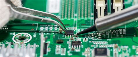
As power electronics continue to evolve, many modern systems require printed circuit boards capable of handling significantly higher current levels without overheating or performance degradation.
A High Current PCB is specifically engineered to carry elevated current loads through optimized copper thickness, reinforced trace design, and enhanced thermal management strategies. These PCBs are commonly used in industrial equipment, automotive systems, renewable energy solutions, and high power control modules.
Unlike standard PCBs, high current boards are designed to minimize voltage drop, prevent excessive heat buildup, and ensure long-term operational stability.
Key Design Features of High Current PCB
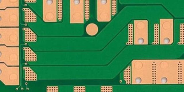
1. Thick Copper Layers
High current PCBs typically use:
-
2oz to 20oz copper thickness
-
Heavy copper internal layers
-
Reinforced power planes
Thicker copper reduces resistance and improves current carrying capacity while maintaining electrical stability.
2. Optimized Trace Width and Spacing
Proper trace width calculation is critical in high current design. Wider traces reduce resistance and heat generation.
Design considerations include:
-
Current load calculation
-
Ambient temperature
-
Allowable temperature rise
-
Safety clearance
Accurate engineering ensures safe operation under continuous heavy load conditions.
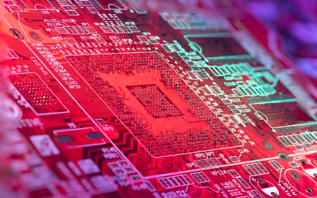
3. Enhanced Thermal Management
High current flow generates heat. Effective heat dissipation is achieved through:
-
Thermal vias
-
Copper pours
-
Heat sinks
-
Metal core substrates (if required)
-
Heavy copper planes
Thermal optimization prevents hot spots and extends product lifespan.
4. Low Resistance and Voltage Drop Control
Power distribution efficiency depends on minimizing:
-
Resistive losses
-
Parasitic inductance
-
Uneven current distribution
Well-designed power planes and reinforced interconnections help maintain stable voltage output across the board.
5. Strong Mechanical Reliability
High current PCBs often operate in harsh environments such as:
-
Automotive engine compartments
-
Industrial control cabinets
-
Renewable energy systems
-
Battery charging stations
Robust lamination and plating processes ensure mechanical durability under thermal cycling and vibration.
Typical Applications of High Current PCB
High current PCBs are widely used in:
-
Power supply units (PSU)
-
DC-DC converters
-
Battery management systems (BMS)
-
Electric vehicle (EV) control modules
-
Solar inverters
-
Industrial motor drives
-
High power LED systems
-
Welding and industrial automation equipment
In automotive and EV systems, stable high current performance is critical for safety and reliability.
High Current PCB vs Standard PCB
| Feature | Standard PCB | High Current PCB |
|---|---|---|
| Copper Thickness | 1oz typical | 2oz–20oz heavy copper |
| Thermal Handling | Basic | Advanced thermal control |
| Current Capacity | Low to moderate | High load capacity |
| Mechanical Strength | Standard | Reinforced structure |
High current PCBs are engineered specifically for power distribution rather than signal routing alone.
Manufacturing Considerations
Producing high current PCBs requires:
-
Accurate copper thickness control
-
Uniform plating distribution
-
Precise etching to maintain trace geometry
-
Strong adhesion between copper and substrate
-
Thorough electrical and thermal testing
Heavy copper processing demands experienced fabrication control to avoid delamination or uneven copper thickness.
Conclusion
High Current PCBs play a vital role in modern power electronics and industrial systems. With thick copper layers, optimized trace geometry, and advanced thermal management, they provide safe and stable performance under heavy electrical loads.
For applications involving high power, energy conversion, or automotive electronics, a well-designed high current PCB ensures long-term reliability and operational efficiency.
