Flying Probe Testing in Small Batch PCB Manufacturing: Precision, Flexibility, and Cost Efficiency
Introduction
In the fast-evolving world of PCB manufacturing, small batch and prototype production demand not just precision, but agility. When fixture-based in-circuit testing (ICT) proves too costly or time-consuming, Flying Probe Testing (FPT) provides an intelligent alternative.
At KKPCB, we integrate fixtureless flying probe systems into our advanced manufacturing lines—enabling rapid setup, accurate diagnostics, and comprehensive electrical validation for low-volume PCB production.
What Is Flying Probe Testing?
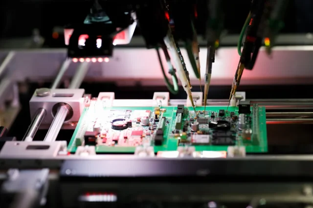
Flying Probe Testing is an automated, software-controlled process used to verify the electrical integrity of printed circuit boards without the need for custom fixtures.
Instead of a static bed-of-nails test fixture, movable probes “fly” across the PCB, contacting designated test points to evaluate connectivity, component orientation, and circuit continuity.
Core Testing Capabilities:
-
Open/short detection
-
Resistance and capacitance measurement
-
Diode and transistor verification
-
Component presence and polarity validation
FPT systems can analyze hundreds of test points per minute with micron-level accuracy—ideal for R&D verification, prototype validation, and low-volume production where agility is critical.
Why Choose Flying Probe Testing for Low-Volume Manufacturing
1. No Fixture Investment
Traditional ICT testing requires expensive, design-specific fixtures that can cost $5,000–$15,000 and weeks to build.
Flying Probe Testing eliminates that cost entirely—ideal for startups, engineering trials, and product revisions.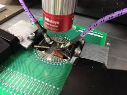
2. Rapid Setup and Turnaround
Once PCB Gerber or CAD files are imported, the system generates the testing sequence automatically.
This enables same-day setup and testing, reducing design-to-validation time from weeks to hours.
3. Flexible for Frequent Design Changes
Every design iteration or layout change can be tested immediately—no retooling required. This adaptability makes FPT invaluable for IoT devices, medical electronics, and automotive prototypes where designs evolve quickly.
4. Cost-Effective for Small Batches
While per-board testing may range from $10–$50, the absence of tooling costs and reduced engineering overhead make FPT economically superior for runs under 500 units.
How Flying Probe Testing Works
1. Design Data Input
Engineers upload Gerber or ODB++ design files containing pad coordinates and test parameters.
The system interprets this data to create a virtual test plan.
2. Probe Movement
Motorized probes—typically four to eight—move simultaneously across the PCB, guided by software to contact specific nodes. Each contact point is verified through precision motion control.
3. Electrical Validation
The system measures:
-
Continuity (open/short verification)
-
Resistance (milliohm-level accuracy)
-
Capacitance and inductance
-
Diode and polarity orientation
4. Data Analysis
The software compiles results into a test report that highlights defective nets, missing components, or parameter deviations.
This data supports early fault correction before boards reach final assembly.
Flying Probe Testing vs. In-Circuit Testing
| Aspect | Flying Probe Testing (FPT) | In-Circuit Testing (ICT) |
|---|---|---|
| Setup Cost | No fixtures required | High fixture cost ($5,000–$15,000) |
| Setup Time | 1 day or less | 2–3 weeks |
| Best For | Prototypes, small batches | Mass production |
| Speed | Slower per board | Faster for large volumes |
| Flexibility | Easy to modify for new designs | Requires new fixture |
| Accuracy | High for connectivity and component tests | Comprehensive functional testing |
Economics of Flying Probe Testing
-
Upfront Cost: Minimal – no fixtures or hardware setup
-
Testing Time: 5–15 minutes per board (depending on complexity)
-
Batch Efficiency: Ideal for 10–500 unit runs
-
Long-Term ROI: Significant cost savings for companies producing varied designs or frequent prototypes
For small manufacturers and R&D teams, this method offers the best balance of cost, precision, and speed.
Applications of Flying Probe Testing
-
Prototyping: Quick validation for design verification before full-scale production.
-
Low-Volume Production: Perfect for customized electronics, IoT devices, and high-mix PCBs.
-
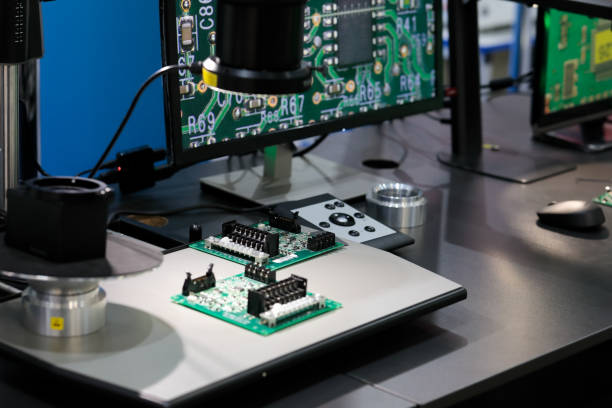
Design Validation: Detects signal integrity issues and layout errors early in development.
-
Complex Boards: Verifies fine-pitch, HDI, and multi-layer designs with precision.
Limitations to Consider
-
Testing Speed: Slower for high-volume production (>1,000 units).
-
Signal Coverage: Limited for ultra-high-speed (>1 GHz) circuits.
-
Per-Unit Cost: Higher than mass testing, though offset by fixture savings.
For medium-to-high volume production, hybrid approaches—combining FPT for prototypes and ICT for scaling—can offer optimal efficiency.
Optimizing FPT for Maximum Efficiency
-
Design for Testability (DFT): Include accessible test points (≥2 mm spacing).
-
Collaborate Early: Work closely with your manufacturer to define test parameters upfront.
-
Batch Strategically: Combine similar designs for grouped testing sessions.
-
Analyze Results: Use FPT data to refine future layouts and prevent recurring faults.
Conclusion: KKPCB’s Expertise in Low-Volume PCB Testing
Flying Probe Testing represents the perfect intersection of flexibility and precision for today’s low-volume PCB manufacturing.
At KKPCB, we deploy advanced flying probe systems that enable fixtureless, high-accuracy testing—ensuring every prototype and small batch PCB meets the same reliability standards as full-scale production.
Whether validating a first prototype or producing small series runs, KKPCB’s integrated test process guarantees:
-
Faster validation cycles
-
Reduced NPI costs
-
Reliable, repeatable test accuracy
From concept to certification—KKPCB ensures your PCB performs perfectly, every time.
