Harsh-environment IoT gateways—used in industrial automation, outdoor base stations, energy systems, mining networks, and smart transportation infrastructure—operate under extreme thermal stress and wideband RF loading. These platforms demand stable impedance, low-loss transmission, and high-temperature RF reliability to maintain continuous connectivity across Sub-6 GHz, C-Band, and mmWave IoT communication channels.
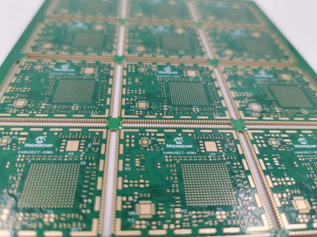
Multilayer HF PCB architectures, built with high-frequency laminates, controlled dielectric parameters, and thermally robust via structures, form the electrical backbone of these gateways. When engineered correctly, these HF PCBs deliver tight impedance windows, stable phase characteristics, and consistent S-parameter performance—even during prolonged exposure to heat, vibration, high humidity, and fluctuating power loads.
High-Temperature RF Reliability—Why It Fails Without Proper HF PCB Engineering

IoT gateways placed in industrial zones or outdoor enclosures encounter temperature cycles ranging from –40°C to +125°C. Under these conditions, standard FR-4 or mid-grade materials lose dielectric stability, causing impedance drift, rising insertion loss, and degraded RF linearity.
Key reliability risks include:
• Thermal expansion mismatch (CTE drift) leading to micro-via fatigue
• Dielectric constant variation destabilizing the impedance of RF traces
• Increased dielectric loss (Df) causing output-power degradation in RF stages
• Phase delay inconsistency across multilayer routing channels
• EMI vulnerability due to insufficient isolation and uncontrolled current return paths
Harsh-environment IoT systems cannot tolerate these failures. This is why multilayer HF PCB designs rely on low-loss materials, balanced stackups, and thermally reinforced via architectures to preserve RF integrity.
Material Science: HF Laminates Designed for Wideband Stability
High-frequency materials used in multilayer HF PCB architectures—such as RO4835, RO4350B, and advanced PTFE-hybrid laminates—offer the dielectric stability required for wideband IoT operation.
Typical HF laminate characteristics:
• Dk stability across –40°C to +150°C maintains impedance consistency
• Df ≤ 0.003–0.004 at 10 GHz ensures low insertion loss for long RF channels
• Thermal conductivity ~0.6 W/m·K improves power-handling capability
• Moisture absorption <0.05% preserves phase stability in humid outdoor deployments
• Low CTE values (10–16 ppm/°C) prevent delamination and maintain via integrity
These properties are crucial for reducing propagation delay variance and preserving multi-band performance.
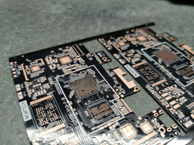
Multilayer HF PCB Architecture—How Reliability Is Engineered
A modern harsh-environment IoT gateway typically requires:
• 6–12-layer HF PCB stackups with alternating microstrip/stripline RF channels
• Controlled dielectric thickness (±3–5 μm) to ensure ±5% or tighter impedance windows
• Smooth-foil copper to minimize conductor losses at high frequencies
• Thermally reinforced via arrays for stable current distribution
• Shielded ground structures for wideband EMI suppression
These engineered features work together to provide uniform propagation constants, reduced mode conversion, and minimized RF distortion.
Routing Optimization for Wideband RF Stability
High-speed routing in IoT gateways must retain S-parameter consistency across wide frequency ranges. Techniques include:
• Phase-matched differential pairs to stabilize multi-band transceiver signals
• Grounded coplanar waveguide (GCPW) for controlled impedance in exposed environments
• Tuned stub lengths and back-drilled vias to suppress resonances
• Tight coupling control to mitigate crosstalk in dense RF clusters
These routing optimizations reduce insertion loss, maintain group-delay uniformity, and improve multi-channel RF coherence.
Thermal and Mechanical Reinforcement for Harsh Environments
To prevent high-temperature failure, the multilayer HF PCB must be mechanically stabilized through:
• Filled and capped microvias to reinforce interlayer reliability
• High-Tg prepregs to resist thermal cycling fatigue
• Embedded thermal vias under PA/LNA regions to dissipate RF heat
• Low-warpage stackup balancing for stable connector alignment
These mechanical strategies ensure long-term dimensional stability and RF consistency.
EMI/EMC Architecture: Ensuring Gateway Stability in Noisy Environments
Harsh-environment IoT gateways operate near motors, power converters, and RF-interfering equipment. EMI suppression is engineered through:
• Segmented ground planes to confine return currents
• RF fences and stitching vias to prevent lateral energy leakage
• Localized cavity shielding for transceiver and LO generation blocks
• Optimized reference plane transitions to reduce mode conversion
Together these features maintain clean EM fields, improving receive sensitivity and uplink/downlink reliability.
Reliability Validation for Industrial IoT Deployment
A complete reliability suite includes:
• Thermal cycling (–40°C ↔ +125°C) to test impedance stability
• High-humidity exposure (85°C / 85% RH) to assess Dk/Df drift
• Vibration and shock testing to ensure mechanical integrity
• High-power RF endurance tests to monitor insertion-loss stability
• Reflow cycling to validate multilayer stackup robustness
Passing these tests verifies that the HF PCB maintains low-loss, phase-stable performance over years of continuous outdoor operation.
Engineering Summary
Multilayer HF PCB architectures are indispensable for harsh-environment IoT gateways. By combining low-loss dielectric materials, thermally reinforced stackup engineering, precision impedance control, and EMI-optimized layouts, these PCBs deliver the:
• high-temperature RF reliability
• ultra-tight impedance stability
• consistent wideband transmission
• superior noise immunity
required for next-generation industrial IoT systems.
