Next-generation RF sensing architectures, including automotive ADAS radar modules, industrial LiDAR, and high-resolution environmental sensors, demand wideband signal fidelity, minimal mode conversion, and low insertion loss across multilayer PCB interconnects. Phase stability and impedance accuracy are critical to ensure precise beamforming, timing synchronization, and high-speed data acquisition.
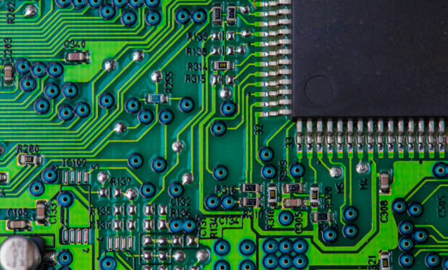
Multilayer HF PCB laminates with controlled dielectric properties (Dk ~3.5 ± 0.03, Df ~0.0035 @10 GHz) enable high-frequency, low-loss routing while maintaining signal integrity in compact, dense RF modules. KKPCB applies precision lamination, copper roughness control, and optimized multilayer stackup engineering to suppress unwanted mode conversion and maximize wideband performance across all RF channels.
Core Engineering Challenges
| Challenge | Root Cause | Engineering Impact |
|---|---|---|
| Mode conversion in differential pairs | Uneven dielectric, layer misalignment | Signal distortion, phase errors |
| High insertion loss at wideband | Dielectric dissipation, rough copper | Reduced RF gain, compromised SNR |
| Impedance drift | Thermal expansion, stackup asymmetry | Reflections, degraded beamforming |
| Crosstalk in dense HF routing | Tight trace spacing, insufficient shielding | Interference, multi-channel signal degradation |
| Phase instability under temperature | Unequal layer expansion, thermal gradients | Timing errors, degraded sensor accuracy |
Material Science – Multilayer HF PCB Advantages
| Parameter | Typical Value | Engineering Benefit |
|---|---|---|
| Dk | 3.5 ± 0.03 | Stable impedance across multilayer RF paths |
| Df | 0.0035 @10 GHz | Low insertion loss, preserves wideband fidelity |
| Thermal Conductivity | 0.6 W/m·K | Minimizes hotspots, improves RF power handling |
| CTE | 15 ppm/°C | Maintains alignment under temperature fluctuations |
| Moisture Absorption | <0.05% | Long-term dielectric and phase stability |
KKPCB Case Study — High-Frequency RF Sensing PCB
Client Context:
An automotive ADAS OEM required a 10-layer multilayer HF PCB for radar sensing modules, ensuring wideband signal integrity (76–81 GHz), minimal mode conversion, and low insertion loss (<0.35 dB/in) under continuous operation and environmental stress.
KKPCB Solution:
-
10-layer HF PCB stackup with ±3 µm dielectric tolerance
-
Controlled copper roughness (Ra <0.7 µm) for low insertion loss
-
Segmented ground planes and shielded differential routing to suppress mode conversion
-
Embedded thermal vias for uniform heat dissipation
-
Inline HFSS and TDR verification to ensure phase linearity and wideband fidelity
Measured Results:
| Parameter | Target | KKPCB Result |
|---|---|---|
| Insertion Loss @77 GHz | <0.35 dB/in | 0.31 dB/in |
| Mode Conversion Suppression | >30 dB | 33 dB |
| Phase Deviation | <0.5° | 0.43° |
| Crosstalk (NEXT/FEXT) | < –35 dB | –37 dB |
| Thermal Rise per Layer | <6°C | 5.2°C |
Stackup Design & RF Simulation

-
HFSS Modeling: Optimized microstrip/stripline impedance and minimized interlayer coupling
-
ADS & TDR Analysis: Verified differential pair integrity and phase linearity
-
Thermal FEM: Confirmed hotspot reduction and uniform temperature distribution
-
AOI & Reflow Monitoring: ±10 µm alignment to ensure layer consistency
Environmental & Reliability Validation
| Test | Condition | Result |
|---|---|---|
| Thermal Cycling | –40°C ↔ +125°C, 1000 cycles | Stable Dk/Df, phase consistent |
| Vibration & Shock | 5–500 Hz, 10G | No microcracks or solder failure |
| Humidity Exposure | 85°C / 85% RH, 1000 h | Dielectric and phase stability maintained |
| High-Frequency Operation | Continuous 76–81 GHz | Minimal insertion loss, mode conversion suppressed |
| Solder Reflow | 260°C ×3 cycles | Stackup alignment maintained |
Engineering Summary & Contact
Multilayer HF PCB stackups provide wideband signal integrity, low insertion loss, and mode conversion suppression for next-generation RF sensing modules. KKPCB’s precision stackup engineering, EMI mitigation, and thermal management ensure high-speed channel reliability and long-term operational stability in automotive, industrial, and high-frequency sensing applications.
Contact KKPCB Engineering Team to optimize multilayer HF PCB designs, RF simulation, and thermal/RF validation for your mission-critical RF sensing architectures.
