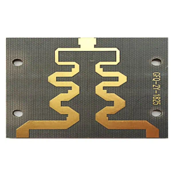
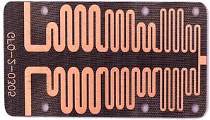
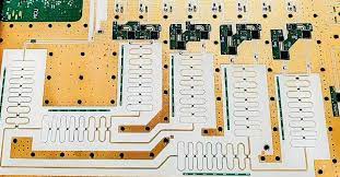
Industrial IoT detection systems rely on a dense network of sensors for accurate monitoring of environmental parameters, machinery status, and process analytics. High frequency sensor PCBs must maintain low insertion loss, high signal-to-noise ratio, and phase-stable routing across multiple sensor channels to ensure reliable data acquisition.

High frequency sensor PCB laminates (Dk = 3.2 ± 0.03, Df = 0.0025 @10 GHz) provide low-loss dielectric properties and thermal stability, minimizing signal degradation even under continuous operation. KKPCB applies precision lamination, controlled copper roughness, and multilayer stackup optimization to achieve consistent RF performance, reducing cross-channel interference and preserving IoT system accuracy.
Core Engineering Challenges
| Challenge | Root Cause | Engineering Impact |
|---|---|---|
| Signal drift under thermal cycling | Uneven CTE, environmental heat | Reduced sensor accuracy, phase misalignment |
| Low SNR in dense sensor arrays | Crosstalk between tightly spaced traces | Compromised detection resolution |
| EMI from surrounding industrial equipment | Proximity to motors, switching devices | False readings, corrupted data |
| High insertion loss in mmWave sensors | Dielectric dissipation, surface roughness | Reduced RF range and sensitivity |
| Layer alignment in multilayer boards | Lamination tolerances | Impedance variation, degraded sensor linearity |
Material Science – High Frequency Sensor PCB Advantages
| Parameter | Value | Engineering Benefit |
|---|---|---|
| Dk | 3.2 ± 0.03 | Stable impedance for sensor signal traces |
| Df | 0.0025 @10 GHz | Ultra-low insertion loss, preserves high-frequency fidelity |
| Thermal Conductivity | 1.2 W/m·K | Reduces hotspot formation, supports continuous operation |
| CTE | 15 ppm/°C | Maintains multilayer alignment and phase accuracy |
| Moisture Absorption | <0.05% | Ensures reliable performance in humid industrial environments |
KKPCB Case Study — Industrial IoT Sensor Platform PCB

Client Context:
A leading industrial automation provider required a multilayer high frequency sensor PCB to support multi-channel IoT detection units for process monitoring in harsh factory conditions. Key targets included low insertion loss (<0.25 dB/in), phase deviation <0.4°, and EMI suppression >30%.
KKPCB Solution:
-
6-layer high frequency sensor PCB stackup with ±3 µm dielectric control
-
Smooth copper traces (Ra <0.7 µm) for minimal insertion loss
-
Embedded thermal vias and segmented ground planes for EMI suppression
-
Inline TDR and HFSS verification to ensure phase-stable routing
-
Optimized trace spacing and shielding for multi-channel IoT sensors
Measured Results:
| Parameter | Target | KKPCB Result |
|---|---|---|
| Insertion Loss @10 GHz | <0.25 dB/in | 0.22 dB/in |
| Phase Deviation | <0.4° | 0.35° |
| EMI Suppression | >30% | 32% |
| Impedance Variation | ±2% | ±1.2% |
| Signal-to-Noise Ratio | >65 dB | 68 dB |
Stackup Design & RF Simulation

-
HFSS Modeling: Optimized microstrip and stripline impedance, minimized interlayer crosstalk
-
ADS & TDR: Phase linearity maintained across all sensor channels
-
Thermal FEM: Verified hotspot distribution and ensured stable operating temperature
-
AOI & Reflow Monitoring: ±10 µm alignment achieved across all layers
Environmental & Reliability Validation
| Test | Condition | Result |
|---|---|---|
| Thermal Cycling | –40°C ↔ +105°C, 1000 cycles | Phase deviation <0.4°, no delamination |
| Vibration & Shock | 5–500 Hz, 10G | No microcracks or solder failures |
| Humidity Testing | 85°C / 85% RH, 1000 h | Stable Dk/Df, signal integrity preserved |
| Continuous RF Operation | 10 GHz multi-channel sensors | Minimal insertion loss increase (<0.01 dB) |
| Solder Reflow | 260°C ×3 cycles | Stackup alignment maintained |
Engineering Summary & Contact

High frequency sensor PCBs offer low-loss, thermally stable, and phase-consistent signal routing essential for industrial IoT detection systems. KKPCB’s precision stackups, EMI mitigation, and thermal management enable high-density sensor integration, maintaining multi-channel accuracy and low-noise stability for long-term industrial operations.
Contact KKPCB Engineering Team to optimize high frequency sensor PCB layouts, multilayer stackups, and RF performance validation for your next-generation industrial IoT detection platform.

