Engineering Precision: The Critical Role of Probe Card PCBs in Semiconductor Testing
Introduction
In semiconductor production, precision defines success. Every chip must be verified for performance and reliability before it’s packaged—and the key to this process lies in the probe card PCB.
At KKPCB, we specialize in engineering high-performance probe card PCBs that ensure accurate, repeatable, and reliable wafer-level testing. These boards bridge the test system and wafer through microscopic electrical connections, enabling early defect detection and process optimization.
What Is a Probe Card and How Does It Work?
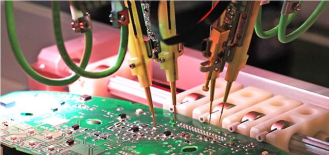
A probe card is an electromechanical interface that connects a semiconductor wafer to a test system. It allows engineers to evaluate the electrical performance of integrated circuits before packaging, reducing waste and improving yield.
At the heart of every probe card is a precision-engineered PCB, responsible for signal routing, impedance control, and electrical stability across thousands of microscopic contact points.
Core Components Include:
-
Probes (Needles or Cantilevers): Ultra-fine contacts that touch wafer pads to transmit signals.
-
Probe Card PCB: Routes signals from probes to the test equipment while maintaining minimal loss.
-
Support Frame: Provides mechanical alignment and stability under repeated testing cycles.
Step-by-Step: Wafer Testing Process 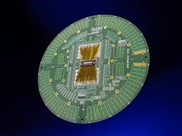
-
System Setup & Calibration
The probe card is mounted on the probe station, and alignment is calibrated with sub-micron precision. -
Wafer Loading & Alignment
The wafer is placed on the chuck and positioned so that each die aligns perfectly beneath the probe array. -
Probe Contact
The probes gently touch the wafer bond pads to establish reliable electrical connections. -
Electrical Testing
Test signals are transmitted through the probes to evaluate voltage, current, resistance, and switching behavior. -
Data Analysis & Yield Reporting
Non-conforming dies are identified early, ensuring only functional chips proceed to packaging.
This process, known as wafer probing, is critical to ensuring device reliability before mass production.
Why Probe Card PCBs Are Indispensable
1. Precision Electrical Contact
Each integrated circuit contains micron-scale bond pads, demanding precise contact without pad damage. Probe card PCBs maintain stable contact pressure and alignment through advanced materials and microfabrication.
2. High-Frequency Signal Fidelity
Modern semiconductors require multi-GHz validation. KKPCB probe card PCBs utilize low-loss dielectrics and impedance-controlled routing to ensure accurate high-speed signal transmission with minimal reflection or delay.
3. Customization for Every Chip Design
Every wafer layout differs. KKPCB designs custom probe card PCBs tailored to each device’s pin configuration, ensuring exact alignment and signal isolation even in dense pad geometries.
4. Durability for Millions of Cycles
Probe cards must endure millions of landings without degradation. Our PCBs employ reinforced copper layers, tungsten-based probe tips, and diamond-like coatings to maximize lifespan and test stability.
5. Material Innovation
Through the use of advanced laminates and bonding materials, KKPCB ensures minimal signal distortion, high thermal stability, and consistent contact resistance—even in extreme test conditions.
Technological Advancements in Probe Card PCB Design
MEMS-Based Probes
MEMS (Micro-Electromechanical Systems) technology allows for sub-micron probe alignment, essential for next-generation chips with ultra-dense pad arrays.
Laser Micro-Machining
Laser precision enables ultra-fine probe tip geometries that minimize pad wear and maintain consistent contact quality.
Finite Element Analysis (FEA)
KKPCB utilizes FEA simulations to optimize both mechanical flexibility and electrical conductivity, preventing over-stress or thermal warping during high-load testing.
Automated Calibration & Testing
Every KKPCB probe card undergoes automated electrical calibration, ensuring that each unit meets global semiconductor test standards for accuracy and repeatability.
Types of Probe Cards
| Type | Structure & Use | Advantages | Limitations |
|---|---|---|---|
| Needle-Type Probe Cards | Fine metallic needles for general testing | Cost-effective, simple maintenance | Limited precision for high-density designs |
| Vertical Probe Cards | Vertically aligned probes for direct pad contact | High accuracy, great signal integrity | Higher manufacturing complexity |
| MEMS Probe Cards | Micro-machined probes for fine-pitch applications | Superior precision, durability | Higher cost and fabrication difficulty |
Challenges and KKPCB’s Engineering Solutions
| Challenge | KKPCB Solution |
|---|---|
| Miniaturization | Photolithographic probe fabrication and precision alignment |
| High-Frequency Signal Loss | PTFE-based low-loss PCB materials and impedance-matched routing |
| Mechanical Fatigue | Durable alloys and advanced reinforcement coatings |
| Custom Layouts | CAD-driven adaptive probe mapping |
| Contact Stability | Force-controlled alignment systems and closed-loop calibration |
Conclusion
The Probe Card PCB represents the most sophisticated interface in semiconductor testing—where microns define success and stability defines yield.
At KKPCB, we combine materials science, RF engineering, and precision mechanics to deliver probe card PCBs that guarantee accuracy, repeatability, and long-term reliability in every test cycle.
As semiconductors advance toward AI, 5G, and high-density integration, KKPCB continues to push the limits of probe technology, ensuring that every chip tested meets the standards of the future.
