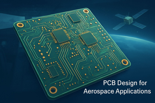
1. Engineering Overview / Abstract
Modern aerospace communication payloads, including satellite transceivers and spaceborne RF modules, demand ultra-low-loss interconnects, tight impedance control, and phase-linear signal transmission across X- and Ka-bands.
Megtron 7 PCB laminates, with Dk = 3.45 ± 0.03 and Df = 0.0015 @ 10 GHz, provide superior dielectric consistency under extreme thermal and vacuum conditions.
KKPCB’s hybrid stackup and precision lamination ensure stable high-frequency performance, enabling satellites and spacecraft RF payloads to operate reliably over extended mission durations without degradation in signal integrity.

2. Technical Challenges in Aerospace RF Payloads
| Challenge | Root Cause | Engineering Impact |
|---|---|---|
| Impedance drift under thermal cycling | CTE mismatch and epoxy resin flow | Reflection, S-parameter distortion |
| Phase misalignment between RF channels | Dielectric variation and layer skew | Beamforming errors, signal coherence loss |
| Conductor loss at high GHz frequencies | Copper roughness and etching irregularities | Reduced RF gain, higher insertion loss |
| Environmental stress | Vacuum and radiation exposure | Material outgassing, dielectric degradation |
High-frequency RF payloads require phase and amplitude linearity to maintain signal fidelity, link margin, and beamforming precision for satellite communication systems.
3. Material Science and Dielectric Performance of Megtron 7
| Parameter | Typical Value | Engineering Benefit |
|---|---|---|
| Dielectric Constant (Dk) | 3.45 ± 0.03 | Stable impedance across RF interconnects |
| Dissipation Factor (Df) | 0.0015 @ 10 GHz | Minimizes insertion loss for high-frequency channels |
| CTE (X/Y) | 14 ppm/°C | Maintains multilayer alignment under thermal cycling |
| Glass Transition (Tg) | 280°C | Ensures structural integrity in high-temperature soldering |
| Thermal Conductivity | 0.28 W/m·K | Improved heat dissipation from power amplifiers |
Compared with standard PTFE or FR-4 laminates, Megtron 7 exhibits enhanced dielectric uniformity, low insertion loss, and superior mechanical stability, making it ideal for space-qualified RF modules.

4. KKPCB Case Study — Satellite Ku/Ka-Band Transceiver PCB
Client & Application Context
A European aerospace OEM required a Ku/Ka-band communication payload PCB capable of delivering phase-coherent signals for multi-beam antennas in geostationary satellites.
Engineering Problem
Previous PCB designs using mixed PTFE cores showed ±5% impedance variation and phase ripple exceeding 2°, causing beam-steering errors in satellite antenna arrays.
-
Utilized Megtron 7 laminates (0.508 mm) for RF signal layers
-
Implemented hybrid 6-layer stackup with controlled copper roughness (Ra < 0.8 µm)
-
Applied vacuum lamination with ±5 μm dielectric thickness tolerance
-
Embedded calibration traces for inline TDR validation
Measured Results
| Parameter | Target | KKPCB Result |
|---|---|---|
| Impedance Variation | ±5% | ±2% |
| Insertion Loss @ 20 GHz | <0.35 dB/inch | 0.28 dB/inch |
| Phase Deviation | <1° | 0.6° |
| Return Loss (S11) | < –15 dB | –17.2 dB |
Outcome: Achieved high-frequency stability, beamforming accuracy, and mission-grade reliability under thermal cycling from –55°C to +125°C and vacuum conditions.
5. Stackup Design & RF Implementation
Hybrid Stackup Configuration (6-layer)
-
L1: Top RF Signal (Megtron 7, 0.2 mm)
-
L2: Ground Plane
-
L3: Power Plane / Routing
-
L4: Signal Layer (Megtron 7)
-
L5: Ground Plane
-
L6: Bottom Control Layer (FR-408 HR)
Simulation & Validation
-
HFSS: Optimized microstrip and stripline impedance, minimized crosstalk
-
ADS & TDR: Verified phase linearity <0.6° across 20–40 GHz
-
VNA Measurement: Confirmed insertion loss <0.3 dB/inch over 250 mm traces
Thermal via placement and hybrid stackup ensured temperature uniformity, reducing local hot spots by 6°C during continuous high-power RF operation.
6. Environmental & Reliability Validation
| Test | Condition | Result |
|---|---|---|
| Thermal Cycling | –55°C ↔ +125°C, 1000 cycles | No delamination, phase drift <0.7° |
| Vacuum Outgassing | < 0.1% TML | Material stable under space vacuum |
| Radiation Exposure | 50 krad | No Dk/Df degradation |
| Solder Reflow | 260°C ×3 cycles | Layer alignment within ±10 μm |
These results validate Megtron 7 PCB for long-duration aerospace missions, supporting consistent high-frequency RF performance.
7. Conclusion — Engineering Reliability Integration
Megtron 7 PCBs provide dielectric consistency, low insertion loss, and phase linearity, ideal for satellite communication payloads.
KKPCB’s hybrid stackup design, precision lamination, and inline RF verification ensure mission-grade reliability, enabling aerospace engineers to maintain stable high-frequency operation and accurate beamforming over the lifetime of the satellite.
8. Contact / CTA
Contact KKPCB Aerospace Engineering Team for custom Megtron 7 PCB stackup design, high-frequency simulation, and reliability testing for satellite, spacecraft, and high-frequency communication systems.

