As semiconductor devices move toward higher speed, finer pitch, and greater integration, wafer-level testing demands extreme precision. The Custom Probe Card PCB forms the electrical backbone of probe card assemblies, enabling accurate signal transmission between automated test equipment and devices under test (DUTs) on the wafer.
A well-designed custom probe card PCB directly impacts test accuracy, yield, and repeatability.
What Is a Custom Probe Card PCB?
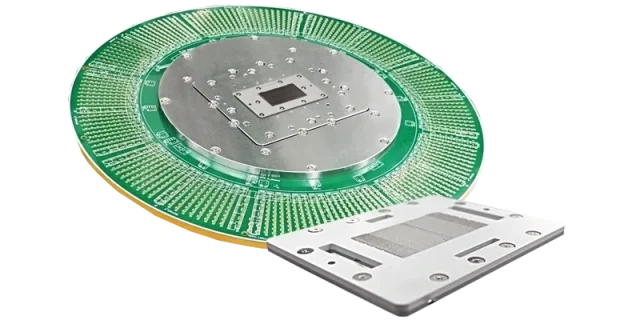
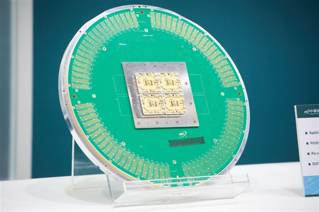
A Custom Probe Card PCB is a highly specialized printed circuit board used within probe card systems for wafer-level semiconductor testing. It provides electrical routing from probe needles or MEMS probes to the ATE interface while maintaining strict signal, power, and mechanical requirements.
Each probe card PCB is customized for a specific device, test platform, and performance target.
Why Customization Is Essential for Probe Card PCBs
Standard PCB designs cannot meet the demands of wafer probing. Custom probe card PCBs are engineered to:
-
Match exact pad layouts and pitch
-
Support ultra-high pin counts
-
Meet specific impedance and timing requirements
Customization ensures reliable contact and accurate measurements.
Signal Integrity for High-Speed Wafer Testing
High-speed probe card testing requires:
-
Controlled impedance routing
-
Low-loss materials
-
Minimal via stubs and discontinuities
Custom probe card PCBs are optimized to preserve signal integrity from probe tips to test instruments.
Power Integrity and Noise Isolation
Stable power delivery is critical for accurate wafer testing. Custom probe card PCBs incorporate:
-
Dedicated power and ground planes
-
Short, low-inductance current paths
-
Noise isolation between analog and digital domains
These measures reduce test variation and false failures.
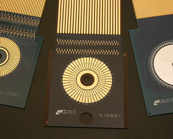
High Density and Fine-Pitch Routing Capability
Probe card PCBs often require:
-
Extremely fine trace widths and spacing
-
High layer count or HDI structures
-
Precise via placement
Advanced fabrication technology is essential for consistent results.
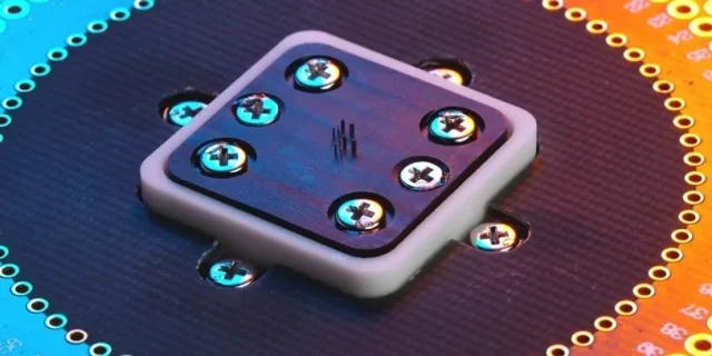
Mechanical Precision and Structural Stability
Beyond electrical performance, probe card PCBs must maintain:
-
Flatness and coplanarity
-
Mechanical stability during probing
-
Compatibility with probe card fixtures
Mechanical accuracy ensures consistent probe contact across the wafer.
Manufacturing Challenges and Quality Control

Producing custom probe card PCBs involves:
-
Tight fabrication tolerances
-
Precise layer alignment
-
Comprehensive electrical testing and inspection
Experienced manufacturing is key to achieving reliable performance.
Typical Applications of Custom Probe Card PCBs
Custom probe card PCBs are widely used in:
-
Wafer-level IC testing
-
Logic, memory, and RF device probing
-
Advanced node semiconductor characterization
-
High-speed and mixed-signal testing
Each application requires tailored PCB solutions.
Choosing a Custom Probe Card PCB Manufacturer
When selecting a custom probe card PCB supplier, consider:
-
Proven experience with semiconductor test PCBs
-
Capability for high-density and controlled impedance designs
-
Engineering support for SI/PI optimization
-
Small batch and NPI manufacturing flexibility
The right partner ensures accuracy and long-term reliability.
Conclusion
The Custom Probe Card PCB is a critical component in modern wafer-level semiconductor testing. By delivering precise routing, stable signal integrity, and mechanical accuracy, custom probe card PCBs enable reliable testing and improved device yield.
Partnering with an experienced custom probe card PCB manufacturer ensures consistent performance from engineering validation through production deployment.
