Wafer-level semiconductor testing demands extreme accuracy, mechanical stability, and signal fidelity. The Custom Probe Card PCB serves as the core interconnect platform between automated test equipment and semiconductor wafers, enabling precise electrical contact and repeatable measurements.
A professionally manufactured custom probe card PCB is essential for high-yield wafer testing.
What Is a Custom Probe Card PCB?
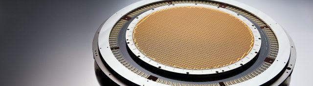
A Custom Probe Card PCB is a highly specialized printed circuit board designed to support probe needles, MEMS probes, or vertical probe structures. It interfaces directly with semiconductor wafers to enable parametric, functional, and reliability testing.
Why Custom Probe Card PCBs Are Critical
Probe card applications require:
-
Extremely fine pitch and tight tolerances
-
Stable electrical characteristics across temperature cycles
-
High mechanical precision for repeatable probing
Customization ensures exact alignment with wafer pad layouts.
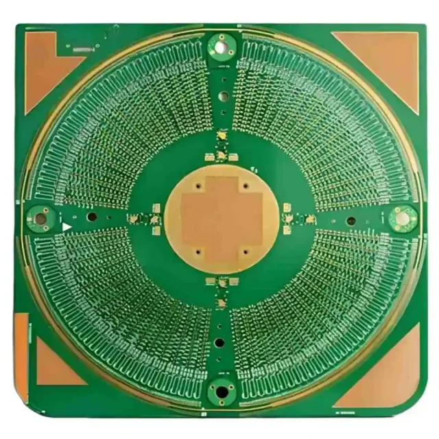
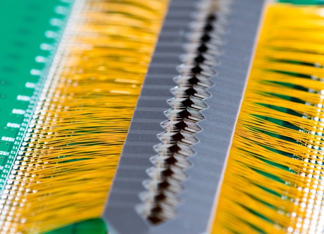
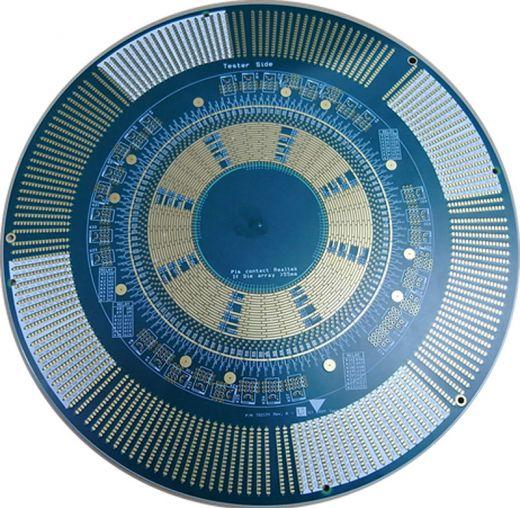
Ultra-Fine Routing and High-Density Interconnect
Custom probe card PCBs often incorporate:
-
Fine-line and fine-space routing
-
HDI and microvia structures
-
High pin count interconnects
These technologies support dense signal channels and precise probe alignment.
Signal Integrity at the Wafer Interface
Maintaining signal integrity is critical for accurate measurements. Custom probe card PCBs focus on:
-
Controlled impedance transmission lines
-
Short, symmetrical signal paths
-
Low parasitic capacitance and inductance
These features minimize signal distortion at high frequencies.
Power Distribution and Grounding Strategy
Stable power and grounding are essential. Custom probe card PCBs typically use:
-
Dedicated power and ground planes
-
Low-inductance current paths
-
Ground shielding around sensitive signals
Proper grounding reduces noise and improves measurement repeatability.
Mechanical Stability and Flatness Control
Probe card PCBs must maintain:
-
Excellent flatness across the board
-
Dimensional stability under thermal stress
-
Robust mechanical support for probe structures
Precision manufacturing ensures consistent probe contact.
Material Selection for Probe Card PCBs
Material choice impacts both electrical and mechanical performance. Common options include:
-
High-Tg FR-4 for structural stability
-
Low-CTE materials for dimensional control
-
Hybrid laminates for high-frequency testing
Careful material selection enhances long-term reliability.
Manufacturing Challenges and Quality Control
Fabricating custom probe card PCBs requires:
-
Tight registration and alignment accuracy
-
Reliable microvia formation
-
Advanced inspection and electrical testing
Strict quality control ensures consistent wafer-level performance.
Applications of Custom Probe Card PCBs
Custom probe card PCBs are widely used in:
-
Wafer-level semiconductor testing
-
IC parametric and functional testing
-
High-frequency and mixed-signal devices
-
Advanced logic and memory testing
Each application demands precision and reliability.
Choosing a Custom Probe Card PCB Manufacturer
When selecting a custom probe card PCB supplier, consider:
-
Experience with wafer-level test boards
-
HDI and fine-line manufacturing capability
-
Controlled impedance and signal integrity expertise
-
Support for prototype and low-volume production
A specialized manufacturer ensures reliable probe card performance.
Conclusion
The Custom Probe Card PCB is a mission-critical component in wafer-level semiconductor testing. Through ultra-fine routing, precise mechanical control, and stable electrical performance, custom probe card PCBs enable accurate and repeatable wafer testing.
Partnering with an experienced custom probe card PCB manufacturer ensures high yield and long-term reliability in advanced semiconductor test applications.
