Custom ATE PCB: Designing High-Performance Test Boards for Automated Test Equipment
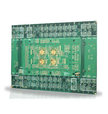
In modern electronics manufacturing, Custom ATE PCB (Automated Test Equipment PCB) plays a crucial role in ensuring product quality, reliability, and performance. A custom ATE PCB is specifically designed for test fixtures or testers that interface with electronic devices under test (DUT). These PCBs provide precise signal routing, robust connections, and optimized layouts for high-speed, high-power, or high-density testing applications.
Custom ATE PCBs are used in industries such as semiconductors, automotive electronics, aerospace, consumer electronics, and medical devices.
What Is a Custom ATE PCB?
A Custom ATE PCB is a printed circuit board tailored for use in automated test equipment. Unlike standard PCBs, ATE PCBs are designed to:
-
Interface accurately with the DUT
-
Provide controlled signal paths for high-speed testing
-
Withstand repeated mechanical connections and probe cycles
-
Support high current or voltage testing if needed
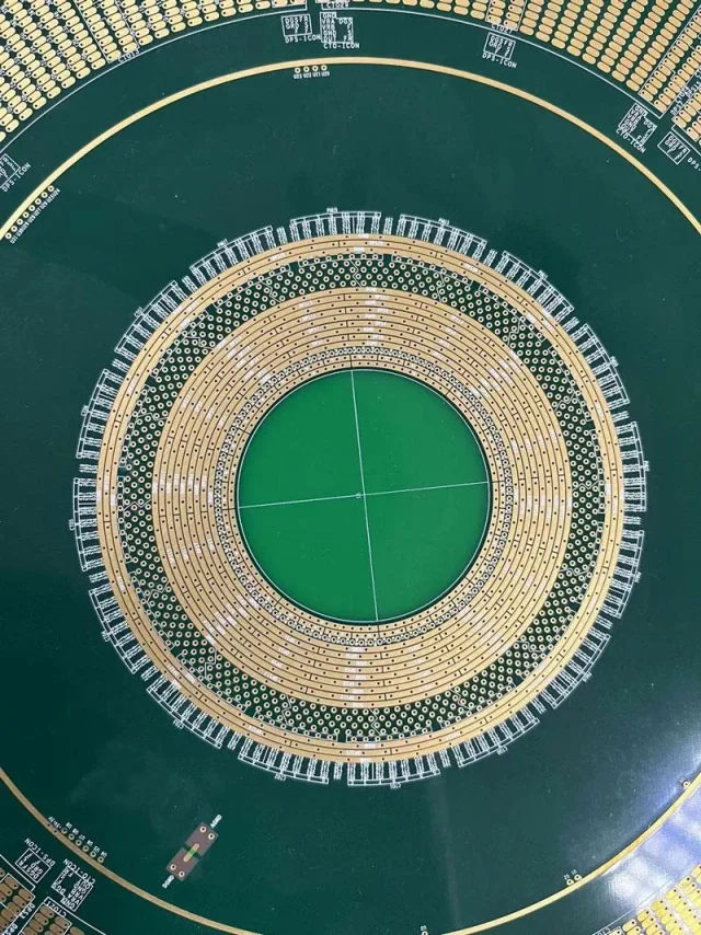
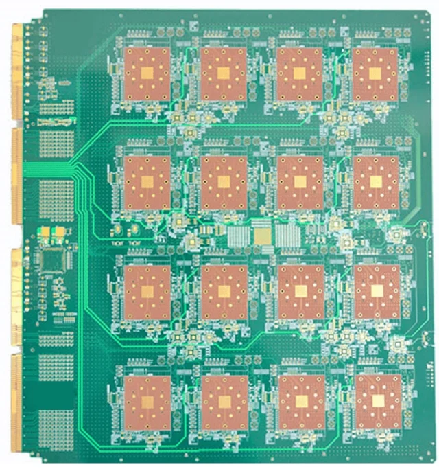
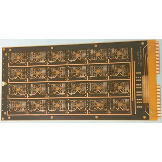
These boards often incorporate multilayer designs, heavy copper layers, fine-pitch traces, and robust connectors to meet demanding test requirements.
Advantages of Custom ATE PCBs
1. Precise Signal Integrity
High-speed or high-frequency testing requires PCBs with controlled impedance and minimal signal distortion.
2. Reliability for Repeated Use
ATE PCBs are subjected to repeated insertion cycles, so materials and layout must ensure long-term durability.
3. Tailored Layouts for Specific DUTs
Custom designs ensure optimal routing, connector placement, and probe accessibility for each device being tested.
4. Support for High-Power or High-Current Testing
Specialized copper thicknesses and thermal management features allow safe testing of power electronics.
5. Flexible Integration with Test Fixtures
Custom ATE PCBs can include mechanical mounting features, alignment pins, and custom connectors for automated test systems.
Design Considerations for Custom ATE PCBs
Designing a reliable custom ATE PCB involves careful attention to:
-
Signal routing and impedance control for high-speed testing
-
Copper thickness and trace width for high-current applications
-
Thermal management to prevent overheating during stress tests
-
Mechanical robustness to handle repeated probe cycles
-
Connector placement and fixture alignment for automated operation
Collaboration with PCB manufacturers ensures the board can withstand rigorous testing and maintain consistent performance.
Applications of Custom ATE PCBs
Custom ATE PCBs are widely used in:
-
Semiconductor testing (ICs, memory chips, processors)
-
Automotive ECU testing
-
Power electronics testing (LED drivers, inverters, motor controllers)
-
Consumer electronics QA (smartphones, tablets, IoT devices)
-
Aerospace and defense electronics testing
-
Medical device testing
In all these applications, a well-designed custom ATE PCB ensures accurate measurements and improves manufacturing yield.
Manufacturing Considerations
Custom ATE PCBs require advanced manufacturing techniques, including:
-
Multilayer PCB fabrication for complex signal routing
-
Heavy copper plating for high-current applications
-
Fine-line or microvia technology for compact high-density layouts
-
High-reliability surface finishes (ENIG, OSP, or HASL)
-
Rigorous testing to ensure consistent performance under repeated cycles
Close collaboration between designers and manufacturers is essential for producing durable and accurate ATE PCBs.
Conclusion
Custom ATE PCBs are essential for modern automated test systems, enabling accurate, reliable, and efficient testing of high-speed, high-power, or high-density electronic devices. By focusing on precise signal routing, thermal management, and mechanical durability, engineers can design ATE PCBs that meet the rigorous demands of modern electronics manufacturing and testing.
