As semiconductor devices continue to evolve toward higher speed, higher integration, and smaller geometries, reliable and accurate testing has become a critical step in the product lifecycle. Chip Test PCBs serve as the essential interface between semiconductor chips and automated test equipment (ATE), enabling precise electrical measurements, functional verification, and performance validation.
A well-designed chip test PCB ensures signal integrity, mechanical stability, and repeatability, helping semiconductor manufacturers improve test accuracy, reduce failure rates, and accelerate time-to-market.
What Is a Chip Test PCB?
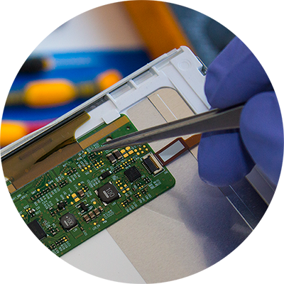
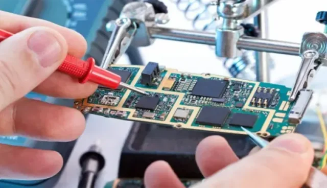
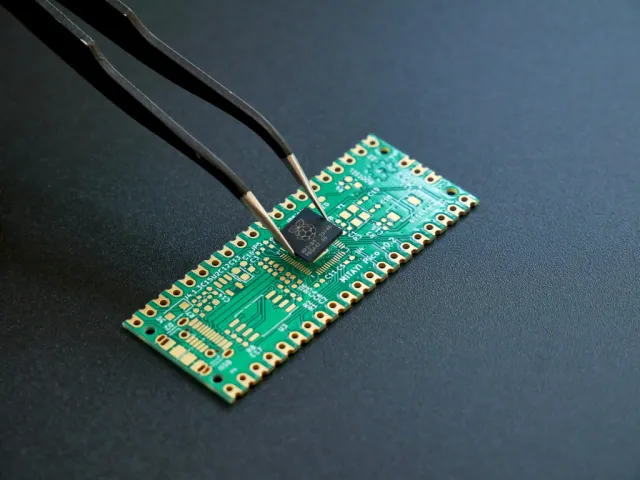
A Chip Test PCB is a specialized printed circuit board used to test semiconductor devices such as ICs, SoCs, memory chips, and RF components. It connects the device under test (DUT) to test instruments through probe cards, sockets, or load boards.
Key functions include:
-
High-density signal routing between chip pads and ATE systems
-
Controlled impedance for high-speed digital and RF signals
-
Mechanical precision for accurate chip or probe alignment
-
Support for high pin count and fine-pitch semiconductor devices
Chip test PCBs are engineered for accuracy, durability, and repeatable performance.
Key Features of Chip Test PCBs
-
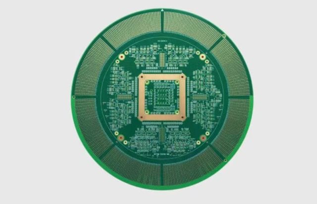
High-Density and High Pin Count Design
Supports modern chips with hundreds or thousands of I/O connections using fine-line routing and HDI technology. -
Controlled Impedance and Signal Integrity
Maintains stable signal transmission for high-speed digital, RF, and microwave chip testing, reducing crosstalk and reflections. -
Multilayer and HDI Stackups
Optimized layer structures separate signal, power, and ground planes to improve electrical performance. -
Mechanical Precision and Reliability
Ensures accurate socket or probe alignment and consistent contact during repeated test cycles. -
Thermal and Electrical Stability
Designed to withstand burn-in testing, high-current operation, and long-duration test conditions.
Materials and Stackup Considerations
Material selection is critical for chip test PCB performance:
-
High-Tg FR-4 for standard digital and memory chip testing
-
Low-loss laminates for RF and high-speed IC applications
-
Hybrid stackups combining FR-4 and RF materials for mixed-signal designs
-
Thermally stable cores to prevent warpage during repeated testing
Proper materials ensure signal integrity, low loss, and dimensional stability throughout the test process.
Applications of Chip Test PCBs
Chip test PCBs are widely used in:
-
IC and SoC functional and parametric testing
-
Memory chip testing (DRAM, SRAM, Flash)
-
RF and microwave chip validation
-
Wafer-level and package-level semiconductor testing
-
ATE systems, load boards, probe cards, and test sockets
These applications require high accuracy, controlled impedance, and reliable mechanical performance, all delivered by professional chip test PCB solutions.
Choosing a Chip Test PCB Manufacturer
When selecting a chip test PCB supplier, consider:
-
Experience in semiconductor test PCB design and fabrication
-
Capability for multilayer, HDI, and high-pin-count PCBs
-
Expertise in controlled impedance and high-speed signal routing
-
Support for prototype, small-batch, and volume production
-
Strong quality control and electrical testing processes
An experienced manufacturer ensures consistent testing results, reduced development risk, and faster validation cycles.
Conclusion
Chip Test PCBs are a critical component of semiconductor testing, providing high-density routing, controlled impedance, and mechanical precision for accurate device validation. Whether used for ICs, memory, or RF chips, a high-quality chip test PCB enables reliable measurements, efficient testing, and a smooth transition from prototype to mass production.
