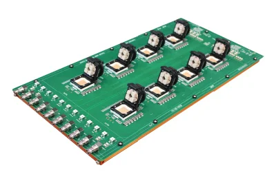
What Is a Burn-in PCB?
A Burn-in PCB is a specialized printed circuit board used for burn-in testing and stress screening, where electronic components or assemblies are operated under elevated temperature, voltage, and current conditions for extended periods. The goal of a Burn-in PCB is to identify early-life failures and improve long-term product reliability.
Burn-in PCBs are widely used in semiconductor manufacturing, automotive electronics, industrial control, and high-reliability systems.
Key Requirements for Burn-in PCB
A reliable Burn-in PCB must meet strict performance and durability requirements:
-
High temperature resistance
Stable operation at elevated temperatures for long durations. -
High current handling capability
Supports continuous power stress. -
Excellent mechanical strength
Withstands repeated insertion and removal cycles. -
Reliable electrical connections
Ensures stable contact during long test hours. -
Long-term stability and repeatability
These requirements distinguish Burn-in PCBs from standard test boards.
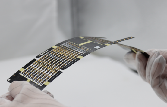
Material Selection for Burn-in PCB
Material choice directly affects Burn-in PCB reliability:
-
High-Tg FR-4 or enhanced epoxy materials
For elevated temperature endurance. -
Heavy copper layers
Support high current paths and heat dissipation. -
Polyimide materials
For extreme temperature and long-term stability. -
Ceramic substrates (Alumina)
For high-power or high-temperature applications.
Material selection depends on test conditions and stress profiles.
Design Considerations for Burn-in PCB
Effective Burn-in PCB design focuses on durability and stability:
-
Wider traces and thicker copper
-
Optimized power distribution
-
Robust via structures
-
Socket and connector reinforcement
-
Thermal management features
-
Redundant grounding and power paths
These design choices ensure safe and reliable stress testing.
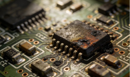
Manufacturing Challenges of Burn-in PCB
Producing a Burn-in PCB requires specialized manufacturing expertise:
-
Consistent copper thickness control
-
High-temperature lamination processes
-
Strong solder mask adhesion
-
Reliable plating and via integrity
-
Extensive electrical testing
Quality issues can lead to test instability or false failures.
Advantages of Professional Burn-in PCB Manufacturing
Partnering with an experienced Burn-in PCB manufacturer provides:
-
Stable performance under extreme conditions
-
Long service life and reusability
-
Reduced downtime during testing
-
Consistent and repeatable test results
-
Support for custom burn-in fixtures
These advantages are essential in production test environments.
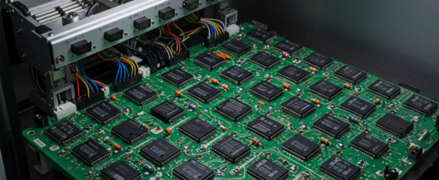
Applications of Burn-in PCB
Burn-in PCBs are commonly used in:
-
Semiconductor burn-in systems
-
IC package and module reliability testing
-
Automotive electronics stress testing
-
Industrial and power electronics validation
-
Production-level quality screening
They play a critical role in ensuring product reliability.
Conclusion
A Burn-in PCB is a critical tool for reliability verification and early-failure detection. By withstanding high temperature, high current, and long operating cycles, Burn-in PCBs help ensure that only reliable products reach the market.
Choosing a qualified Burn-in PCB manufacturer ensures durable design, stable performance, and dependable results in demanding burn-in and stress test applications.
