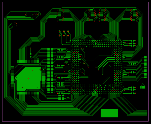
Buried via technology has become essential in modern PCB design, particularly for high-density, high-performance applications. Unlike through-hole vias that pass through all layers, buried vias connect only internal layers, leaving outer layers uninterrupted. This allows designers to maximize routing space, improve signal integrity, and achieve compact, multilayer PCB layouts.
Design Advantages
-
Maximizing Board Real Estate:
By hiding connections within inner layers, buried vias free up external surfaces for additional routing, component placement, and power planes. This is especially beneficial in mobile devices, IoT modules, and compact industrial electronics where space is at a premium. -
Signal Integrity and Performance:
Buried vias reduce parasitic capacitance and inductance compared to through-hole vias, minimizing signal reflection and crosstalk. This is crucial for high-speed digital circuits, RF applications, and mmWave modules where signal integrity directly affects system performance. -
Thermal and Power Considerations:
High-density boards often involve power-intensive components. Buried vias can be strategically placed to act as thermal conduits, improving heat dissipation from inner layers without interfering with outer layers or component placement.
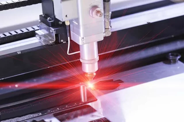
Manufacturing Challenges
Producing buried via PCBs is more complex than standard multilayer boards. Key challenges include:
-
Sequential Lamination: Inner layers must be laminated and drilled in stages, which requires precise layer alignment and process control.
-
Via Filling and Plating: Buried vias often require copper plating and filling to ensure conductivity and reliability, particularly for high-reliability industrial or aerospace applications.
-
Registration and Tolerance Control: Accurate alignment is critical to prevent electrical failure. Any misalignment between layers can lead to short circuits or open connections.
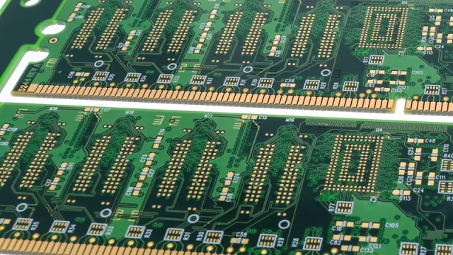
KKPCB utilizes advanced sequential lamination, precise drilling, and plating processes to produce buried via PCBs with high yield and exceptional reliability.
Quality Assurance and Testing
Buried via PCBs demand thorough inspection, as defects inside the layers are not visible from the surface. Common QA methods include:
-
X-ray Inspection: Detects internal defects and ensures via connectivity.
-
Electrical Testing: Confirms continuity and impedance compliance for high-speed signals.
-
Thermal Cycling Tests: Validates reliability under extreme operating conditions.
These measures ensure that buried via PCBs meet the strict standards required for industrial, automotive, and aerospace applications.
Applications of Buried Via PCBs
Buried via technology is widely used in:
-
Mobile and Wearable Devices: Maximizing routing space for miniaturized circuits.
-
High-Speed Communication Modules: Ensuring signal integrity for 5G and networking equipment.
-
Automotive Electronics and ADAS Systems: Supporting compact, high-density sensor networks.
-
Aerospace and Defense Electronics: Providing reliable multilayer connections in demanding environments.
By integrating sophisticated design strategies, precise manufacturing, and comprehensive testing, KKPCB delivers high-quality buried via PCBs that meet the performance, reliability, and space requirements of today’s electronics.
