As semiconductor devices move toward higher speed, higher pin count, and higher integration, testing accuracy has become a key factor in product quality and yield. Automated Test Equipment (ATE) PCBs are at the heart of modern semiconductor testing systems, providing a stable and high-performance interface between devices under test (DUTs) and automated test platforms.
A professionally manufactured ATE PCB ensures accurate signal transmission, repeatable measurements, and long-term reliability across functional testing, parametric testing, and production screening.
Role of ATE PCBs in Semiconductor Testing
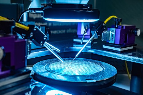
An Automated Test Equipment PCB is designed to support the electrical and mechanical requirements of high-volume and high-precision semiconductor testing. It enables:
-
High-speed signal routing between DUTs and test instruments
-
Stable controlled impedance for digital, analog, and RF signals
-
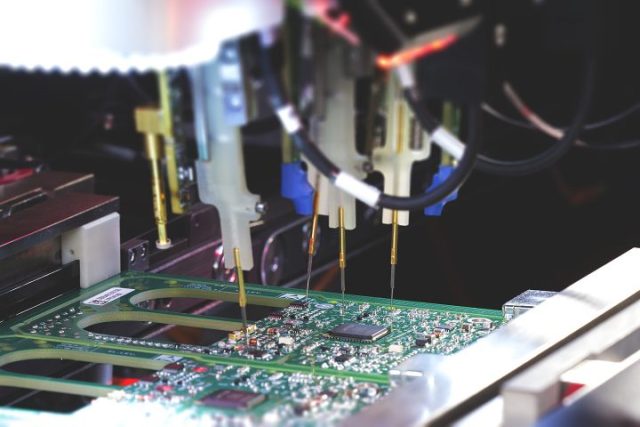
Mechanical support for probe cards, sockets, and load boards
-
Consistent performance over thousands of test cycles
ATE PCBs are essential for maintaining test accuracy, throughput, and system stability.
Key Design Characteristics of Automated Test Equipment PCBs
-
High Pin Count and High-Density Interconnects
Modern ICs and memory devices demand fine-line routing, HDI structures, and multilayer stackups to accommodate complex pin layouts. -
Controlled Impedance and Signal Integrity
ATE PCBs are engineered to minimize crosstalk, reflections, and insertion loss, ensuring accurate high-speed and RF measurements. -
Multilayer Architecture for Noise Control
Dedicated power and ground planes improve signal isolation and reduce electromagnetic interference during testing. -
Mechanical Accuracy and Durability
Tight tolerances maintain precise probe or socket alignment, even under repeated insertion and long test cycles. -
Thermal Stability
Designed to withstand burn-in tests, high-current operation, and temperature cycling without warpage or performance drift.
Material and Stackup Selection
Selecting the right materials is critical for ATE PCB performance:
-
High-Tg FR-4 for standard IC and memory test applications
-
Low-loss laminates for high-speed or RF test environments
-
Hybrid stackups combining FR-4 and RF materials for mixed-signal ATE systems
-
Optimized copper thickness and surface finishes for reliable electrical contact
Proper stackup design ensures stable impedance, mechanical integrity, and long-term test reliability.
Applications of Automated Test Equipment PCBs
ATE PCBs are widely used in:
-
IC and SoC functional and parametric testing
-
Memory testing (DRAM, SRAM, Flash)
-
RF and microwave semiconductor validation
-
Wafer-level and package-level testing
-
Load boards, probe card assemblies, and test socket interfaces
These applications require high accuracy, repeatability, and durability, all of which depend on high-quality ATE PCB manufacturing.
Selecting an Automated Test Equipment PCB Manufacturer
A reliable ATE PCB supplier should offer:
-
Proven experience in semiconductor test PCB manufacturing
-
Capabilities for multilayer, HDI, and high-pin-count PCBs
-
Expertise in controlled impedance and high-speed routing
-
Support for prototype, small-batch, and volume production
-
Comprehensive quality control and electrical testing
Choosing the right manufacturing partner helps reduce test errors, shorten validation cycles, and improve overall testing efficiency.
Conclusion
Automated Test Equipment PCBs are a critical foundation of semiconductor testing infrastructure. With high-density routing, controlled impedance, mechanical precision, and thermal stability, ATE PCBs enable accurate and repeatable testing for ICs, memory devices, RF components, and advanced semiconductor technologies.
Partnering with an experienced ATE PCB manufacturer ensures reliable testing performance, faster development cycles, and smooth scaling from engineering validation to mass production.
