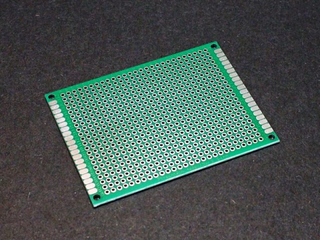
Modern electronics development depends on fast, accurate, and predictable PCB prototype fabrication. As device complexity rises—spanning RF modules, 5G transceivers, AI accelerators, and densely integrated consumer electronics—engineering teams rely on high-precision prototyping to validate architectures before mass production. PCB prototype technology has evolved from simple single-layer boards into a highly automated, material-specific, impedance-controlled manufacturing discipline. The precision gained at the prototype stage directly influences signal integrity, electromagnetic behavior, and long-term thermal reliability.
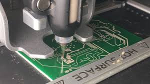
High-precision PCB prototypes begin with accurate copper imaging and fine-line processing. Advanced LDI (Laser Direct Imaging) systems now achieve sub-50 μm line/space capability while maintaining tight registration across multilayer stacks. This resolution enables engineers to design HDI structures, mmWave feedlines, and dense BGA breakout channels without compromising manufacturability. For RF and high-speed applications, such precision reduces conductor loss and stabilizes characteristic impedance, ensuring that early prototypes reflect real operating conditions.
Another essential part of modern PCB prototyping is material-specific process control. Different dielectric substrates—FR-4, high-Tg materials, PTFE laminates, ceramic-filled composites—exhibit distinct thermal expansion, resin flow, and drilling characteristics. Prototype lines must adjust lamination profiles, prepreg flow control, and via metallization chemistry to match the behavior of the chosen substrate. Engineers evaluating low-loss communication systems benefit from accurately processed Rogers or Taconic substrates, where dielectric thickness uniformity directly affects microstrip and CPWG (coplanar waveguide) performance at microwave and mmWave frequencies.
Impedance control is a defining requirement in high-speed PCB prototypes. Differential pairs used in PCIe, USB4, 25–112 Gbps SerDes links, and RF front-end architectures demand controlled dielectric spacing and consistent copper geometry. Prototype fabrication integrates statistical impedance measurement with in-process coupons, allowing real-time adjustments to copper etch factors and laminate tolerances. These measurements provide engineers with early confirmation that simulated signal behavior matches practical hardware performance.
Via technology also shapes prototype accuracy. Laser-drilled microvias, stacked microvia structures, and hybrid buried-via configurations reduce parasitic inductance and shorten interconnect paths. Properly fabricated HDI via structures ensure clean transitions for high-speed lines and stable grounding for sensitive RF modules. Early access to these via technologies lets design teams optimize routing density and evaluate layer-to-layer signal transitions before committing to a production-scale stackup.
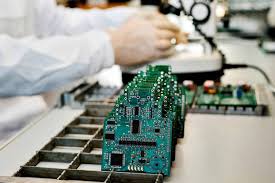
Fast validation cycles depend on inspection and metrology. Automated optical inspection (AOI), X-ray via analysis, and resonance-based impedance measurement ensure that rapid prototypes maintain production-level quality. These inspection systems detect micro-defects—voids, under-etch, smear, misregistration—before they influence electrical performance. The combination of fast turnaround and high inspection accuracy allows engineering teams to run multiple iterations in compressed development windows.
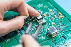
In modern electronics, a PCB prototype is no longer merely a “first attempt.” It is a verification platform where electrical, thermal, and mechanical behaviors converge. High-precision prototype fabrication enables predictable system performance, reduces debug cycles, and strengthens the transition from engineering design to mass production. For companies developing RF communication hardware, high-speed computing units, industrial IoT devices, or complex multilayer assemblies, advanced PCB prototyping technology is now a strategic requirement rather than a convenience.
As complexity continues to rise, the engineering advantage shifts toward teams that can iterate quickly on reliable, metrically controlled hardware. PCB prototype technology, supported by advanced materials, precision equipment, and high-speed fabrication workflows, accelerates innovation and ensures production-ready performance from the earliest stages of design.
