The Importance of Dk/Df Stability in 5G Systems
As 5G communication systems continue to evolve, especially in Massive MIMO radio units, maintaining ultra-consistent dielectric constant (Dk) and dissipation factor (Df) is critical for ensuring stable RF performance and reliable high-speed signal transmission.
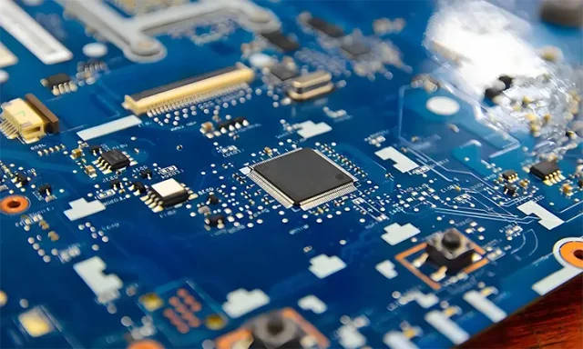
In high-frequency RF PCB design, even small variations in Dk/Df performance can lead to signal distortion, phase imbalance, and reduced system efficiency. This makes advanced materials like RO4835 PCB laminates essential for modern 5G infrastructure.
What is RO4835 PCB Material?
RO4835 PCB material is a high-performance RF laminate designed for high-frequency applications, particularly in 5G base stations and massive MIMO systems.
Key Material Properties
- Low and stable dielectric constant (Dk)
- Ultra-low dissipation factor (Df)
- Excellent thermal stability
- Low insertion loss for high-speed signals
Compared to standard materials, RO4835 PCB provides superior signal integrity and consistency across wide frequency ranges.
Why Dk/Df Consistency Matters in Massive MIMO
In 5G Massive MIMO radio units, multiple antennas operate simultaneously, requiring precise synchronization and phase alignment.
Impact of Dk/Df Variations
- Signal phase mismatch
- Increased insertion loss
- Reduced beamforming accuracy
- Degraded system performance
Using RO4835 PCB engineering, designers can achieve highly consistent Dk/Df values, ensuring optimal RF performance.
Engineering Strategies for Ultra-Consistent Dk/Df Performance
1. Advanced Material Selection
Choosing RO4835 PCB materials ensures:
- Stable dielectric properties over frequency
- Reduced signal variation
- Reliable high-frequency PCB performance
2. Optimized Multilayer PCB Stack-Up
A carefully engineered multilayer PCB stack-up helps maintain consistent electrical characteristics:
- Controlled dielectric thickness
- Stable impedance environment
- Balanced layer symmetry
3. Precision RF PCB Layout Design
Proper RF PCB layout is essential to preserve Dk/Df consistency:
- Uniform trace geometry
- Controlled impedance routing
- Minimized discontinuities
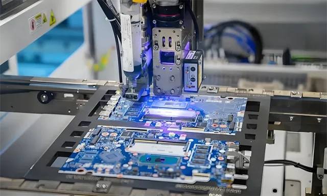
4. Tight Manufacturing Process Control
Consistency in PCB fabrication directly impacts material performance:
- Accurate lamination processes
- Controlled etching tolerances
- High-precision drilling and plating
5. Thermal Stability Management
Temperature variations can affect dielectric performance. Effective thermal design ensures:
- Stable Dk/Df behavior under heat
- Reduced performance drift
- Improved system reliability
Benefits for 5G Massive MIMO Radio Units
By leveraging RO4835 PCB engineering, manufacturers can achieve:
- Ultra-consistent Dk/Df performance
- Improved signal integrity and reduced loss
- Enhanced beamforming accuracy
- Higher efficiency in massive MIMO systems
- Reliable long-term performance in 5G infrastructure
Applications in High-Frequency Communication Systems

RO4835 PCB solutions are widely used in:
- 5G base stations
- Massive MIMO radio units
- RF front-end modules
- High-speed networking equipment
These applications require precise and stable high-frequency PCB performance.
Best Practices for RO4835 PCB Design
To maximize performance, engineers should:
- Carefully select material thickness and configuration
- Optimize PCB stack-up design
- Maintain strict impedance control
- Ensure high-quality fabrication processes
- Conduct thorough RF testing and validation
Conclusion: Enabling Next-Generation 5G Performance
Achieving ultra-consistent Dk/Df performance is essential for the success of 5G Massive MIMO systems. Through advanced RO4835 PCB engineering, manufacturers can deliver high-performance RF PCB solutions that meet the demanding requirements of modern communication infrastructure.
As 5G technology continues to expand, the role of high-quality PCB materials and design expertise will be increasingly critical.
