Looking back and examining the evolution of computing technology, we see that many products widely used in everyday life today have changed significantly over time. Looking back at Apollo workstations, the first PCs, and mainframes that could occupy entire floors of buildings, it becomes clear that miniaturization has been the foundation of technological progress.
Recent innovations in tablets, smartphones, ultrabooks, and other electronics have presented engineers with the complex task of finding a balance between optimal form, size, and functionality. Developers must also consider material, component, and signal/power quality requirements to ensure the new product meets all necessary specifications. One of the key factors in creating electronics that meet these requirements is the use of embedded component technology , which has recently become widespread in aerospace, telecommunications, military, medical, and consumer electronics.
We may not have directly experienced the impact of this process, but we have witnessed the creation of compact cameras and video cameras, small wearable gadgets, and a host of other miniature devices, including tiny electronic devices used in modern medicine. As the cost of producing circuit boards containing embedded components decreases, other industries are also beginning to actively implement this technology, meaning we will soon see a new wave of innovative products on the market. Along with the advancement of embedded component technology, printed circuit board design and manufacturing has also evolved .
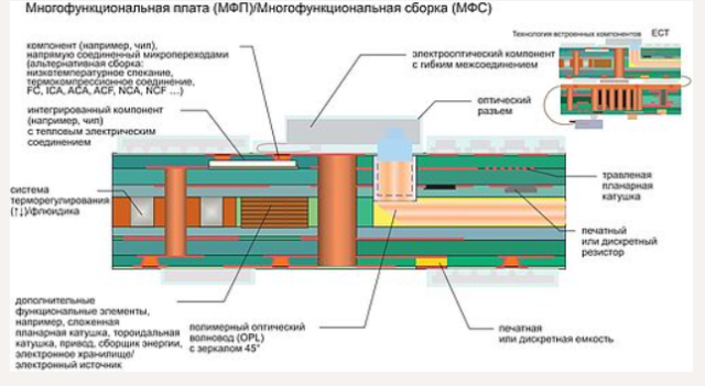
Design companies are working closely with their manufacturers to refine the manufacturing process of multifunctional boards and enclosures, applying cutting-edge technologies to meet growing consumer demands. Some of these boards incorporate electro-optical components with flexible interconnects, integrated optical connectors, and polymer-based optical waveguides. Thus, embedded component technology has rapidly evolved from placing passive and active components in laser-cut cavities on a substrate to assembling high-pin-count chips within a substrate with microvias connecting both sides of the chip to adjacent conductive layers. For advanced PCB manufacturers, this methodology has now become a well-established standard procedure.
Back in 2010, Sharon Starr, director of market research at the IPC Association, said, “Embedded components could transform board manufacturers into chip integrators. The board will become one large component, and developments will result in new technologies that can manage electrostatic discharge. Furthermore, some components will migrate from printed circuit boards to embedded BGAs in semiconductor packages. This trend will further facilitate the convergence of printed circuit boards and semiconductor technologies. And it’s likely that the main developments will occur on the package/wafer side, not on the printed circuit board side.”
The prediction has proven correct: little has changed in printed circuit board (PCB) production over the years, but at the wafer/package level, technology has advanced significantly—for example, chiplets, which combine several individual chips into a single module, have become widespread. Previously, embedded components were used to form or place passive components on the inner layers of printed circuit boards. However, with the constant push toward miniaturization of electronics, the industry continues to seek new ways to implement embedded components. We are already seeing manufacturers mass-producing boards with embedded processors, including the use of complex SiP (system-in-package) devices on boards designed to expand the capabilities of product form factors. But before using embedded components in new designs, it is important to understand their specific features, which can impact the entire design. Let’s take a closer look at the advantages and disadvantages of embedded components.
Benefits of embedded components
- Reducing the surface area of the outer layer.
- Increased functionality with the same surface area (higher density):
- For example, the number of components in mobile phones increases, but the general limitations of the form factor remain the same.
- Performance Enhancement:
- Shorter traces with reduced inductance allow for increased overall circuit speed;
- routing closer to reference planes to improve signal integrity (SI) performance, or even shaping components into a Faraday cage to reduce sensitivity.
- Potential reduction in overall assembly costs:
- The cost of the PCB itself will be higher, but some of the cost can be offset by the smaller number of components needed for the finished assembly.
- Solution to the problem of heat dissipation on a printed circuit board:
- Using the board structure to dissipate heat.
- Troubleshooting reliability issues:
- Components inside the board are less susceptible to failure if the board experiences bending or deformation.
- Active devices with a large number of pins can be embedded directly into the substrate:
- This will allow the design to be carried out in such a way as to ensure the protection of the intellectual property rights that constitute the design of the electronic device.
Disadvantages of embedded components
- Too many “cheats” are required to implement the project in outdated 2D design tools.
- For molded components, meeting tolerance requirements can be more challenging:
- Pruning can be slow and expensive.
- Achieving design performance from molded (passive) components can be difficult.
- The cost of prototyping is higher.
- Built-in components may be damaged during assembly:
- Repairing or reworking such a board is practically impossible.
- Using multiple crystals increases the number of power rails.
- Potential negative impact on the thermal performance of the system.
- Additional costs are required to obtain bare-dies from IC suppliers or to develop ASIC devices to be placed on the inner layer.
Common Design Issues Using Embedded Components
From a design perspective, board design could be approached as a two-dimensional object, but with the advancement of embedded component technology, electronic design must be assessed as a three-dimensional task. Design teams must work collaboratively and thoughtfully, from the concept stage to manufacturing, with each board and assembly considered not in isolation but as a component of a complete system to ensure the final product is highly reliable, efficient, and manufacturable.
Some of the common issues that arise when working with embedded components include:
- difficulties with high-speed assemblies and their characteristics,
- insufficient understanding of the design rules and implementation of built-in components in the project,
- the need to conduct a preliminary study of the requirements for the manufacture and installation of boards, taking into account the design rules for manufacturing (DFM).
Embedded technology offers significant potential for high-performance, miniaturized, low-power, and low-cost electronics, but it also requires more precise and stringent design rules, higher clock rates, and lower core and I/O voltages.
Furthermore, when using embedded components, it is important to ensure proper control of thermal conditions and electrical interference, which requires the engineer to address the problem of dissipating large amounts of heat, dealing with increased electrical noise, and ensuring high signal quality.
When selecting components for embedding, the following should be taken into account first:
- body type;
- housing material (for built-in passive devices);
- requirements for a high-speed device;
- overall size, including total number of contacts and die size;
- the distance or pitch between pins in the selected form factor;
- thermal effects;
- price.
These factors influence the choice of component embedding method, as well as the PCB layout (stack).
Devices without a case
One solution for high-speed devices is to use open-die technology, where the die is embedded directly onto the printed circuit board. Open-die technology is most commonly used in multi-chip modules (MCMs) or chip-on-board (COB) assemblies.
The advantages of this technology allow for reduced manufacturing costs and board space savings, while simultaneously reducing the device’s size and volume. This approach also addresses some of the challenges associated with high-speed packages, such as the increasing number of inputs/outputs and increased power dissipation.
Die stacking can also be performed using unpackaged devices. This process involves stacking dies of comparable sizes together and then connecting them using through-silicon vias (TSVs), which are most commonly found in dense system-in-package (SiP) devices. Etching and metallization processes are performed during vertical stacking. This ensures optimal connections between chips and helps improve overall electrical and thermal performance. It also minimizes signal trace lengths, improving signal rise times and reducing trace inductance, ensuring improved electromagnetic compatibility (EMC) in the design.
Consumer demand continues to push manufacturers to create smaller, faster, and smarter digital devices, and direct chip embedding technology can help meet current and future market demands.
Placement of active components
Design challenges often stem from the need to increase the functionality of an existing device while maintaining its current size. When considering next-generation smartphone designs or wearables such as smartwatches or smart glasses, one must ask: how will we continue to meet all functional, electrical, and mechanical requirements within such a small footprint?
This is where we come to the need for advanced technologies like SiP or package-on-package (PoP) , which can reduce board space and be used on both rigid and flexible circuit boards. For example, some component suppliers produce specialized low-profile components that are more suitable for embedding into the printed circuit boards of the latest devices.
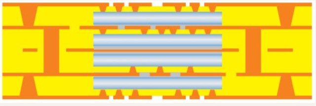
Other innovations in embedded component technology include inserting SiP assemblies into a substrate (Fig. 3) and placing active components with cutouts on base layers within a stack (Fig. 4) by stacking multiple prepreg layers with cavities cut out for the components. Prepreg layers are stacked until all components are covered with the required clearances. Pressure and heat then cure the prepreg layers surrounding the components, creating a new core. These cores with embedded components can then be used as building blocks for subsequent printed circuit board assembly.
There are two main methods for connecting active components in the inner layers of a printed circuit board.
The first method involves soldering the component directly to the conductive layer. This approach is proven and technologically feasible, but there is a risk that the solder will melt during subsequent manufacturing steps.
The second method involves placing the active component between conductive layers directly within the laminate and connecting to the conductive layers via a laser-cut microvia. The advantage of this method is that the connection is made on both sides of the integrated circuit, minimizing the integrated circuit’s footprint and maximizing the number of pins for the device. This improves input/output routing and component routing , as well as reducing the overall trace length for improved signal performance. However, the potential risk of damage to the embedded component during laser drilling of blind vias or during their metallization must be considered.
Design rules for embedded components
Before designing a printed circuit board with embedded components, you need to ensure your CAD tools are suitable. Previously, boards with embedded components were designed using software that only supported 2D images, so engineers who wanted to use advanced assembly technologies faced design challenges and required extensive knowledge and experience to successfully implement their designs. Modern CAD systems are equipped with 3D systems, making the engineer’s job easier and enabling the efficient implementation of embedded components in a board design.
When designing a printed circuit board with embedded components, it is crucial to consider design rules that will help create a product that meets the requirements of all stages from planning to manufacturing and board assembly.
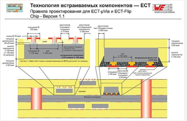
Figure 5 shows an example of the application of design rules using embedded component technology for flip-chip devices and interconnect microvias. This set of requirements, typical for high-density interconnect (HDI) applications with build-up microvias, includes information on pin pitch, pad spacing, and pad width, for example.
Such requirements are typically aligned with the rules implied for layers intended for buildup structures or base layers (core layers). However, this specification may also include specifications for component spacing on inner layers, recommended component thickness, minimum dielectric thickness, and clearance between the adhesive sidewall and the edge of the component package.
This additional information is necessary to account for all the required characteristics for both the internal layers and the Z-axis. This is an example of how properly configured design tools, including the necessary rule sets, can leverage the advantages of 3D systems to create technologically advanced and highly efficient printed circuit boards.
Among other things, when setting design rules, developers should consider:
- actual layers allowed for embedded components,
- installation side,
- the connection strategy used for each layer.
Depending on the manufacturer or assembly materials, engineers may be able to place components on any layer or mount them on any side. Restrictions on the permissible layer or side of the board apply to the placement of embedded components in cutouts.
The designer should work closely with the manufacturer who will manufacture and assemble the board to thoroughly understand the entire process on the shop floor and be able to correctly identify the types of rules required for placement in the CAD library. This will significantly reduce the risk of defects and inconsistencies during production.
It’s also recommended to consider the CAD part library when defining a design rule set for embedded components. In traditional CAD tools, users must define a unique dimension for each layer on which the component will be used. Some systems even require a separate part number for each footprint. This can create a nightmare when attempting to link the information to a corporate PLM/PDM system.
Modern CAD systems make it easy to mark a component both as an SMD component and for embedding on any layer. However, keep in mind that in most cases, you’ll need to create separate footprints for each component, as manufacturing specifications will vary, and you may need to associate two footprints with a part number. Ideally, simply marking the component “for embedding” will be sufficient, and it will be independent of the actual number of layers in the design. If you plan to place the component inside a cavity, you need to define the correct contour and a rule that should be automatically implemented during layout.
Once this work of entering all the necessary rules and creating footprints has been completed, the engineer will have at his disposal a library that precisely meets all the manufacturer’s requirements, which will significantly simplify the process of developing subsequent board designs with embedded components.
Implementation of embedded component technology into the project
To launch a board into production, a large volume of detailed technical documentation must be prepared to avoid errors and ensure the board is manufactured as intended. That’s why the effective implementation of embedded components in a project begins at the product planning stage.
Most project teams have a systems architect who begins the development of a product concept by collecting data on the requirements for the future product from various sources, such as the company’s CEO or CTO, marketing engineers, industrial engineers, and other specialists.
The system architect then uses standard tools available on their PC to outline the general details of the new product. These tools include spreadsheets, presentation slides, text documents, flowcharts, and drawing tools.
Unfortunately, most of them were never intended for electronic design. Finding the optimal solution for implementing embedded components requires an actual design file created in a CAD system. Only with such a file is it possible to perform a detailed analysis and select the most effective technology for implementing embedded components.
Based on a precise design of the device being developed, it is possible to estimate the actual area occupied by printed circuit boards and understand how the use of embedded components can save space and improve the functionality of the product.
This information will allow you to find a compromise between all factors and arrive at an optimal solution by making changes to the design and analyzing the results. Furthermore, this approach helps initiate early planning for the next iteration of the project.
A system architect works with all project documentation: 2D and 3D design files, functional block diagrams, and bills of materials (BOMs). They can generate output data for preliminary thermal, electromagnetic, and radiofrequency analyses and exchange information with 3D MCAD systems for collaborative work on mechanical design aspects, such as the product enclosure, which can be useful, for example, for interference analysis.
During the logic design phase, the electronics engineer can take the design data from the planning phase and begin work on the rest of the project. The process engineer will have more information about the stackup details used in the design and will inform the PCB designer and manufacturer about materials and thicknesses. This approach will help address requirements related to impedance-driven signals and other high-speed constraints.
It’s often convenient for the design team to have the manufacturing engineer, among other things, define constraints for embedded components at this stage, specifying, for example, the required layer and footprint to be used during layout. While the PCB designer can certainly also provide this information, having the manufacturing engineer do so can save time during the design process. Furthermore, the manufacturing engineer should attach notes with specific instructions or link images to the schematic design to share with the PCB designer during layout. At this stage of the physical circuit design, detailed layer planning or the placement process for embedded components should begin.
For placement of standard discrete components directly formed or mounted on inner layers, the functionality provided by a traditional 2D CAD system is sufficient. The only thing a designer needs to consider is whether the system provides adequate design rule checks (DRCs) to prevent errors. However, if working with discrete or active components that will be placed on inner layers with potential cutouts, or with components requiring microvia connections, a full-fledged 3D system is more suitable. It provides access to the necessary design rule checks, supports real-time placement, and enables modeling of actual connections on inner layers and management of cavity structures.
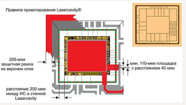
When working with cavity structures, unique shapes may also be required for each layer. It’s important to accurately determine these details, taking into account manufacturer information, and define cavity design rules. An example of such rules is shown in Figure 7. Keep in mind that when working with cutouts and embedding devices with a high pin count, additional space is required for routing on the inner layer, and these aspects must be planned for in advance.
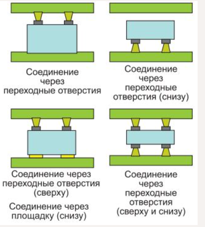
When placing embedded components , it’s crucial to properly design the connection type for them. Since devices can be connected either via pads or microvias on one or both sides, this must be determined and modeled during layout.
The pad and micro-via locations should be communicated to the board manufacturer before fabrication and assembly. This is very easy to do using a 3D system. Using a 2D system, you’ll have to manually extract the center coordinates of each contact or micro-via.
Preliminary production checks and joint work on the results
Although embedded component design guidelines are applied during the development stage, board manufacturers also conduct reviews of incoming designs to ensure the feasibility of manufacturing a particular board. Violating design guidelines can lead to time-consuming and costly rework, and with embedded components, the process becomes significantly more complex.
This is why it’s so important for designers to define fabrication rules (DFM) in the CAD system’s rule database during the design and manufacturing process and to perform checks against these rules during PCB development. PCB manufacturers can typically provide designers with standard manufacturing and assembly rules, as well as requirements specific to specific technologies and equipment capabilities.
It’s important to keep in mind that the requirements for working with embedded components, flexible circuit boards, advanced layouts, or hybrid designs are unique to each manufacturer. Therefore, it’s crucial for the designer to clearly define the rules that apply to the specific board-manufacturer combination.
Manufacturing checks performed during prototyping can be used as part of the product testing process before sending the design to manufacturing. The designer should check with board suppliers to see what formats they support beyond standard Gerber and NC drill files. These formats may include IPC-2581 or ODB++. Using more advanced file formats will save time for both the designer and the manufacturer. To better communicate with the manufacturer, the designer can also create spreadsheets with approval results and graphical snapshots of any issues on the board, if the CAD system they use supports these capabilities.
Using embedded components offers numerous advantages to electronic device designers. When working with embedded components, it’s important to be familiar with existing implementation methods, explore emerging technologies, and thoroughly understand all stages of the design process and the challenges that may arise at each stage of development and manufacturing.
As manufacturing processes improve, developers have ample opportunity to deliver new products with more features in the same or even smaller footprint and, importantly, at the desired cost-effectiveness.
Embedded component technologies are advancing, with cutouts and various connection options becoming increasingly common for devices with high pin counts. To maximize the impact and results from using embedded components, it’s important to begin planning the electronic system at the concept stage and apply all necessary rules throughout the logical and physical design stages and during manufacturing. Using a 3D platform for planning and designing printed circuit boards with embedded components will help you model your design and generate manufacturing output more accurately, saving time throughout the product development cycle.
