Impedance matching in HDI ( High- Density Interconnect ) boards is intended to prevent transmission errors, especially losses caused by transmission line resistance and the dielectric properties of the printed circuit board.
Microvias can be used to create manufacturing-friendly PCB layouts in impedance-matched systems. BGA escape routing and dogbone fanout structures enable impedance matching in HDI PCBs.
When do PCB traces require impedance matching?
Impedance matching is determined not by the signal frequency, but by its slope and rise/fall time. If the signal’s rise/fall time (measured from 10 to 90%) is less than six times the signal propagation delay in the path, the signal is considered high-speed. In this case, precise impedance matching is essential.
The Challenges of Impedance Matching in HDI PCBs
When implementing impedance matching in high-density inkjet (HDI) boards, designers face the following challenges:
- In high-density circuits, components have a reduced pitch between contact pads (e.g., BGA packages). If the BGA pitch is ≤0.65 mm, routing traces and controlling their width becomes challenging. In such cases, via-in-pad and BGA escape routing technologies are used.
- The use of blind vias in the pads avoids the formation of antennas typical of via stubs, thereby improving signal integrity.
- To ensure impedance compliance with signaling standards in HDI controlled impedance boards, careful trace routing and proper stack-up structure are critical.
Designing trace widths for impedance control in HDI
The impedance of a trace is determined by its width and the distance to the reference layer. HDI printed circuit boards with fine-pitch BGA components require careful selection of trace widths and their placement to ensure proper routing between pads and via-in-pads.
Impedance Control for BGA Layout on HDI Boards. High-density assembly (HDI) often involves the use of BGA components. Routing traces from under high-density components with a large pin count requires a special routing strategy. In cases where controlled impedance is essential (for example, for FPGAs and other high-speed components), BGA routing presents particular challenges. The choice of routing strategy is primarily determined by the BGA pin pitch, which sets the maximum allowable trace width between pads. The minimum trace width is also limited by the manufacturer’s process capabilities, stackup, and specified impedance value. When planning the layout, consider the following recommendations:
- For fine-pitch BGA on boards with a medium number of layers, a neck-down method is used at the entrance/exit of the BGA area.
- External conductors can be routed directly to the first row of pads.
- For the second row of BGA pads, the width of the conductors is significantly reduced to accommodate them between the pads of the first row.
- Internal rows are routed using internal layers, typically no more than two rows per layer to control impedance and minimize crosstalk in HDI.
Dogbone wiring
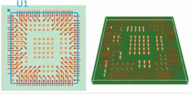
Dogbone routing (a reference to the shape) is the most common method of escape routing and fanout for BGA components (Figure 1).
This technique allows the via to be positioned closer to the pad. There is no need for filling or plating the via, as the component is not soldered directly to the pad containing the via. This method is optimal for BGA assembly with 1mm and 0.8mm pitch.
For BGAs with a pitch smaller than 0.5 mm, microvia-in-pad technology is preferred. In this case, instead of recessing a thin conductor away from the pad, the microvia is placed directly in the contact pad. To prevent solder from penetrating the back of the board, the microvia is filled with conductive compound and copper-plated.
Microvias for BGA pinout
If the contact pad size (including the backplane) is small enough for fine-pitch BGA chips, microvias for routing must be implemented using inner layers. Microvias differ from standard vias in the following ways:
- Via depth. Vias should cross no more than one or two layers. In standard-thickness boards with a higher layer count, vias across more layers are possible, but this will require additional manufacturing processes. Blind and buried vias spanning one layer are recommended.
- Microvia aspect ratio. The optimal depth-to-diameter ratio of a microvia is 0.75:1. For example, for a 32-layer board, the layer thickness (for a two-layer core) is 2 mils (≈50.8 µm), so the via diameter should be no less than 2.7 mils (≈68.6 µm). Mechanical drilling is possible down to 8 mils (≈203 µm), but drill bit breakage is common at this diameter, increasing processing costs to the level of laser drilling. Laser drilling offers higher productivity because it doesn’t require the same safety precautions as mechanical drilling. Switching to laser technology reduces the overall cost of board fabrication.
Dogbone layout guidelines for BGA chips with different pitches
For BGA with 0.8mm pitch:
- conductor width: ≤10 mils (≈254 µm);
- Microvia diameter: ≈6 mils (≈152 µm) (using dogbone fanout).
For BGA with 0.5mm pitch:
- use of filled and plated microvia-in-pad;
- Conductor width: 7-8 mils (≈178-203 µm) to ensure sufficient spacing between adjacent pads.
Microvias in the vertical cross-section can be stacked or staggered to achieve the desired routing density. To ensure reliability, IPC 6012 standard requirements for microvia dimensions and warranty bands must be followed. Microvias in pads are particularly critical for BGAs with a pitch of ≤0.3 mm, where alternative routing methods are not applicable.
How to Place Blind Vias for BGA Routing
Blind vias are a valuable design technique for HDI printed circuit boards, freeing up additional space for routing on inner layers. Compared to through-hole vias, this type of via increases the available routing space on inner layers, allowing for additional traces to connect the pins of inner BGA rows. Figure 2 shows how, on a 1mm-pitch BGA board surface, only two traces can be routed between conventional vias.
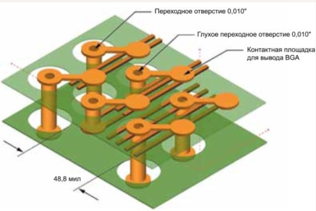
However, using blind vias allows for six traces to be routed underneath them, increasing routing space by 30%. Using this method for routing traces from high-pin-count BGAs reduces the number of required signal layers by a factor of 4. Blind vias are placed in cross-shaped, L-shaped, or diagonal structures, forming so-called boulevards (Fig. 3).
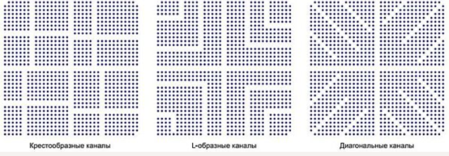
creates “boulevards” on the inner layers, allowing for denser routing. Image source: The HDI Handbook by Happy Holden
The choice of a specific configuration depends on the distribution of the power and ground pins.
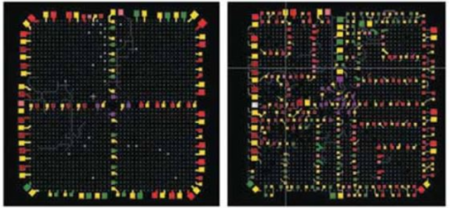
In his book, “The HDI Handbook,” Happy Holden gives an example of a BGA with 1153 pins (34×34, 1 mm pitch), shown in Figure 4.
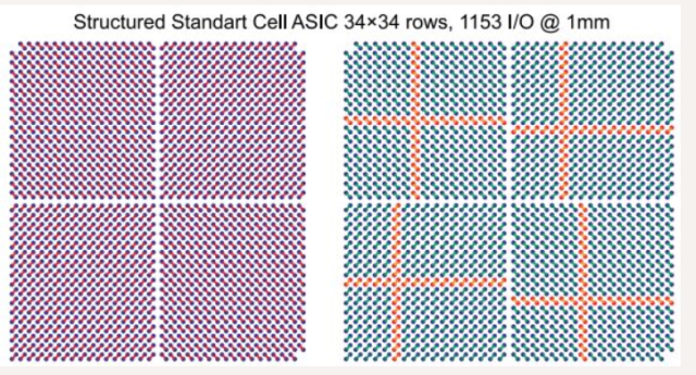
Holden notes, “Each signal layer has 132 possible routing directions (one trace between vias plus 20 traces in crossover channels, five traces each). This means that connecting a given BGA chip to the rest of the circuit requires eight signal layers (plus five shield layers). The vias create a barrier, making routing extremely layer-intensive.”
Happy Holden explains: “Using boulevards increases the number of traces per layer and reduces the overall number of signal layers by creating additional routing space. Blind vias form four cross-shaped boulevards (as shown in the figure). This design provides +48 routing directions per layer (8×6 traces) and improves signal integrity of internal circuits. This eliminates the need for two routing layers and two reference layers.”
He goes on to clarify: “On the back side of the PCB, another advantage of the blind-via boulevards becomes apparent. While the through-hole vias extend across the entire board, the boulevards are now organized within the BGA area.” In Fig. 5 (left): 58 discrete components are connected via 104 vias beneath the BGA. On the right: the boulevards allow 183 components to be connected using 366 shared vias.
One is a traditional quadrant splitter with through-holes,
allowing for the connection of 58 discrete components. The other uses blind vias,
allowing for the connection of 183 discrete components.
Image source: The HDI Handbook by Happy Holden
Length of the wiring section and width of the conductors
Impedance matching is almost always critical when working with high-speed integrated circuits. When analyzing fanout length, it’s important to consider the relationship between layout and impedance control. Due to the length of traces (if any) and the parasitic capacitance/inductance of vias, the fanout of a BGA chip will have its own impedance.
The signal bandwidth should be determined to assess the impact of trace impedance. The trace section within the BGA routing area can be ignored if its length is significantly shorter than the wavelength corresponding to the upper bandwidth limit. The optimal approach is to calculate the load impedance, which is a function of the trace length and the input impedance of the network formed by these traces (after neck-down reduction).
As a rule of thumb, it’s recommended to limit the section length to 10% of the signal wavelength. For a digital signal with a cutoff frequency of 20 GHz, this corresponds to a critical length of 0.73 mm (in a stripline on an FR4 substrate). This means that large integrated circuits, such as FPGAs, will require impedance matching for all circuits—both single-ended and differential pairs.
The key factors are:
- via inductance;
- parasitic capacitance between the board and the contact pad;
- inductance of the IC terminals.
Together, these elements form a T-shaped low-pass filter, where the cutoff frequency of –3 dB represents a typical calculated value for an LC circuit (assuming equal inductance of the via and the IC pin). The T-shaped filter simultaneously performs impedance matching, modifying the output impedance of the driver IC (Fig. 6).
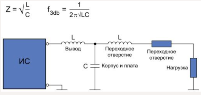
Matching the impedance of a routing path (fanout) is difficult without determining the impedance of the vias connecting the routing traces to the internal layers. However, this can be neglected if the via is short and extends through only a few layers. The total input impedance, including the via and the internal trace, is primarily determined by the impedance of the internal trace when the number of layers involved is small. This is why via impedance is often ignored.
The main drawback is that high-speed BGA components (e.g., FPGAs) may require back drilling to remove the residual via portion beneath the routing area. According to the IPC standard, HDI boards use blind, buried, and laser-directed microvias with a diameter of less than 6 mils (≈0.15 mm), eliminating the need for back drilling and limiting the via inductance only to the thickness of the layers involved.
As the number of layers increases, the layer thickness and the distance to the reference plane decrease, so to maintain the required impedance, it is necessary to reduce the conductor width. For differential pairs, the coupling between the conductors must be taken into account. For precise impedance control, it is recommended to use a CAD system with a built-in electromagnetic field solver, which helps select the optimal conductor width for a given HDI stackup.
Why can’t the width of the path be larger than the size of the landing area?
- The trace width is proportional to its impedance and plays a critical role when operating in HDI mode. Vias become so small that they must be manufactured as microvias as soon as the trace width becomes small enough.
- If the impedance-controlled trace width is excessively wide, you can either reduce the board’s dielectric thickness to reduce the width or increase the contact pad size. From a reliability standpoint, as long as the contact pad size exceeds the value specified in IPC standards, there will be no issues.
- It is recommended to create an impedance profile for the board stackup. After calculating the required width for impedance control, the resulting value should be entered as a design rule. It is advisable to run crosstalk simulations for the proposed trace width to check whether this will result in excessive crosstalk.
Impedance matching in HDI printed circuit boards directly impacts signal quality, so carefully calculated impedance control is essential in such assemblies. The close proximity of components and traces on HDI boards makes this task quite challenging. Using microvias, fine-pitch BGA routing techniques, and fan-out dogbone routing will help designers effectively achieve impedance matching in HDI systems.
