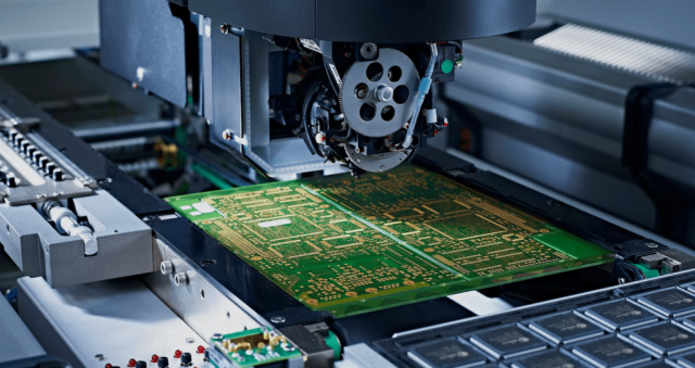
1. Engineering Overview — PCB Reliability in Industrial Wireless Sensor Networks
As industrial IoT systems expand to high-density wireless sensor networks (WSNs), the RF front-end and communication nodes must sustain stable dielectric properties and low signal loss across wide temperature and humidity ranges.
Factories often feature high EMI levels, long sensor link distances, and rapid temperature cycling, which challenge PCB dielectric stability and RF consistency.
KKPCB engineers utilize TLY-5 PCB laminates to achieve:
-
Dielectric uniformity (ΔDk ≤ 0.02) for phase-stable multi-node synchronization
-
Low loss tangent (Df = 0.0009 @10 GHz) to improve energy efficiency in 2.4–5.8 GHz ISM bands
-
Thermal durability that ensures continuous uptime in industrial environments
The TLY-5 platform provides a high-reliability base for smart factories, predictive maintenance systems, and low-power sensor gateways.

2. Technical Challenges in Industrial Wireless PCB Design
Industrial wireless nodes demand RF efficiency, temperature resilience, and signal consistency. FR-4 materials exhibit dielectric variation and energy loss under elevated humidity, causing drift and interference.
| Challenge | Description | Impact |
|---|---|---|
| Dielectric instability | Dk fluctuation with temperature/humidity | Frequency offset, phase delay |
| High insertion loss | Energy dissipation over long trace runs | Reduced transmission range |
| EMI sensitivity | Crosstalk between adjacent antennas | Packet loss, poor reliability |
| Mechanical stress | Vibration & expansion fatigue | Microcrack in plated vias |
By integrating TLY-5 PCB materials into industrial wireless node boards, KKPCB achieves improved dielectric uniformity and superior EMI suppression, extending operational stability across –40 °C to +125 °C.
3. Material Science and Performance Analysis
| Property | Typical Value | Engineering Benefit |
|---|---|---|
| Dielectric Constant (Dk @10 GHz) | 2.20 ± 0.02 | Precise impedance control for RF links |
| Dissipation Factor (Df @10 GHz) | 0.0009 | Low-loss signal transmission |
| CTE (Z-axis) | 46 ppm/°C | Stable through thermal cycling |
| Moisture Absorption | 0.02 % | Maintains Dk uniformity in humidity |
| Thermal Conductivity | 0.45 W/m·K | Efficient heat dispersion from RF amplifiers |
Compared with FR-4, the TLY-5 laminate reduces insertion loss by up to 45% and provides 3× greater phase stability, vital for distributed sensor clock synchronization.

4. KKPCB Case Study — Industrial Gateway PCB for Smart Factory Sensor Network
Project Context:
An industrial automation company needed a 2.4/5.8 GHz dual-band wireless gateway PCB for factory-level WSNs with over 500 sensor nodes.
Requirements included low power dissipation, high RF efficiency, and temperature reliability up to 120 °C.
Engineering Challenges:
-
FR-4 boards exhibited 0.08 dB/cm loss @5.8 GHz
-
Dk drift caused desynchronization across wireless mesh nodes
-
Board warpage after 1000 humidity cycles
-
Substituted FR-4 with TLY-5 0.254 mm core laminate
-
Implemented microstrip impedance control ±3%
-
Optimized ground via placement to suppress EMI
-
Conducted ADS and TDR analysis for impedance linearity
Results:
| Metric | FR-4 Baseline | TLY-5 PCB | Improvement |
|---|---|---|---|
| Insertion Loss @5.8 GHz | –0.08 dB/cm | –0.045 dB/cm | 43.7% lower loss |
| Phase Drift (40–120 °C) | 4.2° | 0.9° | 78% reduction |
| EMI Margin | 12 dB | 23 dB | 11 dB improvement |
| Mesh Sync Reliability | 97.2% | 99.6% | +2.4% stability |
The optimized TLY-5 PCB achieved reliable 24/7 network uptime under vibration, thermal load, and EMI exposure.
5. PCB Stackup and RF Implementation
Hybrid Stackup Configuration (Industrial Wireless Node PCB):
-
L1: RF antenna feed (1 oz rolled Cu)
-
L2: Ground plane
-
Prepreg: FR-408HR 0.1 mm (support layer)
-
L3–L4: Control MCU and power supply
Manufacturing & Validation Process:
-
Controlled lamination @190 °C ±2 °C
-
Copper roughness control (Ra ≤ 1.0 µm)
-
Full TDR impedance mapping
-
5 GHz antenna S11 < –22 dB confirmed via HFSS
Simulation Validation (ADS & HFSS):
-
Insertion Loss: –0.045 dB/cm (5.8 GHz)
-
VSWR < 1.15 across operating band
-
Thermal stability: <1% variation @120 °C
6. Environmental & Reliability Validation
| Test Type | Condition | Result |
|---|---|---|
| Thermal Cycling | –55 °C ↔ +150 °C, 2000 cycles | No Dk drift, no delamination |
| Humidity Aging | 85 °C / 85%RH, 1000 h | ΔDf < 0.00005 |
| Mechanical Shock | 100 g, 6 ms pulse | No via crack or pad lift |
| EMI Stress | 10 V/m RF field | No desense detected |
All validation results confirm industrial-grade RF endurance and long-term dielectric reliability under harsh environmental stress.
7. Engineering Conclusion
The TLY-5 PCB laminate enables high dielectric uniformity, low RF loss, and strong environmental resilience for industrial wireless sensor networks.
Through KKPCB’s controlled lamination and impedance optimization, manufacturers can ensure:
-
Precise phase synchronization across large sensor arrays
-
Energy-efficient data transmission
-
Reliable operation across wide temperature and EMI ranges
TLY-5-based RF boards thus represent an optimal material platform for Industry 4.0 communication systems and wireless IoT gateways.
8. Contact
Contact KKPCB’s RF Engineering Division for material selection, stackup simulation, and RF performance validation of TLY-5 PCB designs used in industrial IoT sensor and gateway systems.

