Why EMC Matters in PCB Design
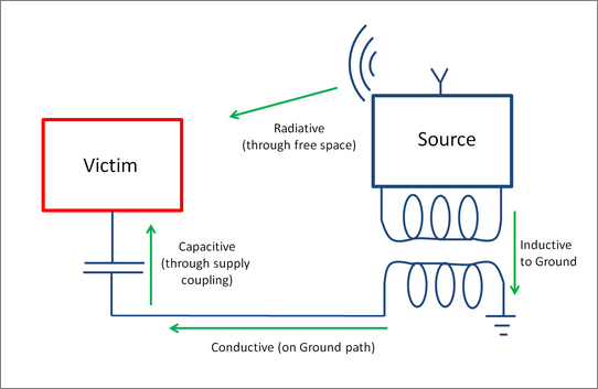
Electromagnetic Compatibility (EMC) is a key requirement in modern PCB design, ensuring that electronic systems operate reliably without generating or being affected by electromagnetic interference (EMI).
Proper PCB layout—especially GND routing, trace spacing, and layer design—plays a decisive role in reducing ESD (Electrostatic Discharge) and improving overall signal integrity.
This article summarizes practical PCB design guidelines compliant with EMC standards, focusing on spacing, grounding, and signal layout strategies.
1. PCB Edge Spacing Specifications
-
Rule: Maintain a minimum spacing of 0.3 mm between the PCB edge (including via boundaries) and any other trace or copper feature.
-
Purpose:
-
Prevents electrical arcing and leakage along board edges.
-
Improves mechanical strength and manufacturing reliability.
-
Tip: Avoid routing high-speed or high-voltage signals near the PCB edge to minimize EMI emissions.
2. Edge GND Trace Layout (Ground Guard Ring)
-
Recommendation: Surround the entire PCB perimeter with a continuous ground (GND) trace or copper pour.
-
Benefit: Acts as an EMC shield, reducing electromagnetic radiation and improving ESD protection.
-
Design Tip: Stitch the edge GND trace with multiple vias (every 10–15 mm) to ensure low-impedance grounding.
3. GND Spacing from Other Traces
-
Spacing Range: 0.2 mm to 0.3 mm
-
Purpose: Balances EMI suppression with routing density.
-
Best Practice: Maintain consistent spacing between GND and signal/power traces to minimize capacitive coupling and noise interference.
4. Power (Vcc) Pin and Trace Spacing
-
Requirement: Keep 0.2–0.3 mm spacing between Vcc lines and adjacent traces.
-
Reason: Reduces the risk of power noise coupling into sensitive signal lines.
-
Tip: Add decoupling capacitors close to Vcc pins to filter transient noise.
5. Spacing for Critical Signal Lines (Reset & Clock)
-
Rule: Maintain ≥0.3 mm spacing between critical signals (such as Reset, Clock, and Oscillator) and other traces.
-
Purpose: Ensures signal integrity, minimizes crosstalk, and prevents timing jitter.
-
Additional Advice: Shield sensitive clock lines with GND guard traces when possible.
6. High-Power Line Spacing Standards
-
Spacing: 0.2 mm to 0.3 mm minimum
-
Considerations:
-
Wider trace width to handle higher current.
-
Adequate spacing for thermal dissipation and safety clearance.
-
Consider thermal relief pads or heat sinks for better temperature control.
-
Tip: Separate high-current paths from low-level signal lines to prevent interference.
7. Multi-Layer GND Via Connections
-
Guideline: Interconnect ground planes across all PCB layers using multiple stitching vias.
-
Purpose:
-
Reduces ground impedance and improves signal return paths.
-
Enhances EMC performance by minimizing voltage differences between layers.
-
-
Best Practice: Place vias near high-frequency signal transitions or at GND plane boundaries.
8. Handling Sharp Corners in Grounding and Routing
-
Issue: Sharp 90° corners act as antenna points, increasing EMI radiation.
-
Solution:
-
Use rounded or 45° chamfered corners instead of sharp angles.
-
Maintain smooth current paths to improve high-frequency signal performance.
-
Bonus Tip: Rounded corners also improve etching precision and PCB manufacturability.
Designing for EMC from the Start
EMC compliance should be integrated into PCB design from the layout stage, not as a post-production fix.
By following these eight key guidelines—covering trace spacing, grounding, and signal routing—you can effectively minimize ESD, EMI, and crosstalk issues, ensuring stable performance and higher product reliability.
