As high-frequency modules continue to evolve in RF communication, radar, and 5G systems, ensuring the performance and durability of RO4350B PCBs has become a critical aspect of RF PCB design and manufacturing. RO4350B PCB laminates, widely used in high-frequency PCB applications, offer low dielectric loss, stable dielectric constant, and excellent thermal performance.
However, achieving optimal performance requires rigorous RF testing and reliability evaluation of RO4350B PCBs. Proper validation ensures signal integrity, impedance stability, and long-term reliability in demanding high-frequency PCB environments.
Overview of RO4350B PCB Material
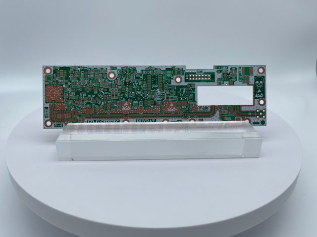
RO4350B PCBs, based on Rogers RO4350B laminates, are engineered for high-speed and RF PCB design. Compared to standard FR4, RO4350B PCB materials provide superior electrical stability and low-loss transmission.
Key properties of RO4350B PCB laminates:
- Low dielectric constant (Dk ≈ 3.48) for controlled impedance PCB design
- Low dissipation factor (Df) for low-loss RF signal transmission
- Excellent thermal stability for high-power RF applications
- Consistent performance across wide frequency ranges
These characteristics make RO4350B PCBs ideal for high-frequency modules and RF systems.
Importance of RF Testing in RO4350B PCB Applications
In high-frequency PCB design, even minor variations can affect performance. RF testing of RO4350B PCBs ensures that the design meets required specifications.
Key objectives of RF PCB testing:
- Validate signal integrity and insertion loss
- Verify impedance control accuracy
- Measure return loss and reflection coefficients
- Evaluate high-frequency transmission performance
Accurate RF testing methods are essential for high-reliability RF PCB applications.
Key RF Testing Methods for RO4350B PCBs
1. Vector Network Analyzer (VNA) Testing
VNA testing is widely used for RF PCB measurement.
Parameters measured:
- S-parameters (S11, S21, etc.)
- Return loss and insertion loss
- Impedance matching performance
This method is critical for validating high-frequency PCB signal behavior.
2. Time Domain Reflectometry (TDR)
TDR testing evaluates impedance discontinuities in RO4350B PCB traces.
Benefits:
- Detect impedance mismatches
- Identify trace defects and discontinuities
- Optimize controlled impedance PCB routing
3. Insertion Loss and Return Loss Measurement
Measuring insertion loss and return loss ensures efficient RF signal transmission in RO4350B PCBs.
- Low insertion loss = better signal transmission
- High return loss = minimal signal reflection
4. Eye Diagram Analysis (for High-Speed Signals)
In mixed RF and high-speed PCB systems, eye diagram testing evaluates signal quality and timing integrity.
Reliability Evaluation of RO4350B PCBs
1. Thermal Cycling Test
Thermal cycling evaluates PCB performance under repeated temperature changes.
- Detects barrel cracking and delamination
- Ensures thermal reliability of RO4350B laminates
2. High-Temperature Storage Test (HTS)
Assesses long-term stability of RO4350B PCBs under elevated temperatures.
3. Humidity and Moisture Resistance Testing
Moisture absorption can affect RF PCB performance.
Testing ensures:
- Stable dielectric properties
- Resistance to environmental degradation
4. Mechanical Reliability Testing
Includes vibration and shock testing for automotive and industrial RF modules.
5. Solder Joint Reliability Testing
Evaluates SMT and through-hole reliability in RO4350B PCBA assemblies.
Design Considerations for Reliable RO4350B PCBs
1. Controlled Impedance PCB Design
Accurate impedance control is essential for RF PCB performance.
2. Optimized PCB Stack-Up
Proper multilayer PCB stack-up design ensures stable electrical behavior.
3. RF Layout Optimization
- Minimize trace length
- Avoid sharp corners
- Reduce via usage
4. Thermal Management
Ensure efficient heat dissipation in high-frequency PCB systems.
5. EMI/EMC Control
Proper shielding and grounding improve RF PCB reliability.
Applications of RO4350B PCBs in High-Frequency Modules
- RF communication systems
- 5G base stations and antennas
- Automotive radar systems
- Satellite communication modules
- High-speed networking equipment
These applications demand high-performance RF PCB testing and reliability validation.
Advantages of RO4350B PCBs
- Excellent low-loss RF performance
- Stable dielectric properties for high-frequency PCB design
- High reliability under thermal and environmental stress
- Consistent signal integrity in RF PCB systems
- Compatibility with advanced multilayer PCB manufacturing
Conclusion
Effective RF testing and reliability evaluation of RO4350B PCBs are essential for ensuring optimal performance in high-frequency modules. By combining advanced RF testing methods with robust PCB design practices, engineers can achieve superior signal integrity, low-loss transmission, and long-term reliability.
For modern RF and high-speed applications, RO4350B PCB laminates provide a proven solution for achieving high-performance and reliable RF PCB systems.
