Building the Backbone of 5G Antenna Performance with RO4350B PCB
- As 5G networks evolve toward higher frequencies (sub-6 GHz → mmWave) and denser integration, PCB performance has become a decisive factor in antenna module design.
Engineers must now balance low insertion loss, thermal stability, and mass-production manufacturability—a challenge only a few materials can meet. - That’s why Rogers RO4350B PCB has become the go-to substrate for 28–39 GHz 5G antenna modules.
It strikes the perfect balance between RF precision, process simplicity, and cost efficiency.
When combined with KKPCB’s high-frequency process control, OEMs can confidently move from RF concept to mass production with repeatable quality.
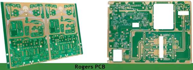
RO4350B PCB
Why RO4350B PCB Excels in 5G Antenna Array Design
- In phased-array antennas, phase consistency across multiple elements defines beamforming accuracy.
Even a 0.02 εr shift can tilt the beam by more than 1°, making material stability—not just dielectric value—essential.
| Property | Typical Value |
|---|---|
| Dielectric Constant (εr @ 10 GHz) | 3.48 ± 0.05 |
| Dissipation Factor (tan δ @ 10 GHz) | 0.0037 |
| Thermal Coefficient of εr | +50 ppm/°C |
| Glass Transition Temperature (Tg) | > 280 °C |
Compared with PTFE-based laminates, RO4350B provides similar RF loss with simpler processing —
no plasma treatment, standard FR-4 drilling, and conventional plating — ideal for high-volume 5G PCB manufacturing.
Case Study: 28 GHz Compact Base-Station Antenna Module
- A global telecom OEM collaborated with KKPCB to develop a 28 GHz phased-array antenna for compact 5G small-cell deployment.
Design Challenges
-
Maintaining impedance tolerance within ± 5 % across multilayer RF stackups
-
Managing thermal drift during hybrid lamination
-
Achieving phase alignment among sub-millimeter antenna elements
KKPCB Engineering Solutions
-
Optimized RO4350B + low-Dk prepreg stackup for thermal balance
-
Applied vacuum lamination to eliminate voids and ensure resin uniformity
-
Used laser-controlled impedance tuning and in-line VNA calibration for array consistency
Results
-
Insertion loss reduced by ≈ 0.17 dB @ 28 GHz
-
Beamforming stability improved by 11 % across temperature range
-
Module yield increased by 9 % after stackup optimization
💡 Engineering Insight:
At 28 GHz, a 0.02 εr deviation shifts the beam by ≈ 1–1.5°.
Through ± 3 °C lamination control and ± 5 µm etching precision, KKPCB achieved repeatable RF performance across production lots.
Design & Manufacturing Best Practices
When designing 5G antenna modules with RO4350B PCB, engineers should focus on:
-
Controlled impedance in microstrip & stripline configurations
-
Smooth copper foils to minimize conductor loss
-
Tight via drilling tolerance (± 0.05 mm) for stable phase control
-
Dielectric and impedance validation for every batch
KKPCB’s 5G Manufacturing Capabilities
-
RF simulation + stackup optimization for multi-array modules
-
± 5 µm precision etching for fine-pitch traces
-
Hybrid lamination with CTE-matched control (< ± 3 °C)
-
Automated impedance verification using calibrated VNA
-
IPC Class 3 & IATF 16949 certified production processes
Why Partner with KKPCB
5G hardware design is more than just choosing a PCB material — it’s about bridging RF design and manufacturability.
KKPCB specializes in high-frequency hybrid PCB manufacturing for telecom, radar, and satellite systems, combining:
-
Multi-material RF stackup design & simulation
-
In-house VNA-based impedance & loss testing
-
Controlled hybrid lamination (RO4350B + FR-4 + ceramic)
-
Qualification documentation (PPAP, IMDS, AEC-Q)
By integrating engineering co-design into manufacturing, KKPCB helps OEMs shorten validation cycles, reduce yield risk, and achieve faster time-to-market for 5G products.
Conclusion
RO4350B PCB delivers the electrical precision, mechanical stability, and scalability required for high-performance 5G antenna array modules.
With KKPCB’s engineering expertise and process discipline, your 5G RF design can move smoothly from prototype to automotive-grade mass production — without compromise.
- Ready to optimize your next 5G antenna module?
Our RF engineering team can help you: -
Select the optimal stackup & material combination
-
Validate impedance / insertion loss in real time
-
Accelerate qualification for market deployment
- Contact KKPCB Engineering Support to discuss your next 5G antenna PCB project or request a DFM review.
