Ensuring PCB Reliability Through Burn-in Testing — How KKPCB Guarantees Long-Term Performance
In high-performance electronics, reliability isn’t a luxury — it’s a requirement. At KKPCB, every printed circuit board that leaves our production line is expected to perform consistently under demanding real-world conditions. One of the most critical steps in achieving that standard is our Burn-in Testing process.
What Is Burn-in Testing?
Burn-in Testing is a controlled stress test applied to PCBs to identify latent defects before deployment. Boards are subjected to elevated temperatures and electrical loads over a defined period to simulate real-world operational stresses.
This process accelerates potential early-life failures — often called the infant mortality phase — ensuring only the most stable, reliable boards proceed to final shipment.
Why Burn-in Testing Matters
Modern PCBs power mission-critical systems — from telecommunications and industrial automation to automotive and aerospace electronics. Any early failure can result in costly downtime or safety risks.
By integrating Burn-in Testing into the manufacturing flow, KKPCB ensures that hidden material defects, soldering inconsistencies, or marginal components are detected early — not in the field.
The KKPCB Burn-in Process
Our Burn-in Testing is designed with precision, repeatability, and data integrity at its core:
-
Preparation & Board Selection
Representative samples from each production batch are selected based on product type and application requirements. -
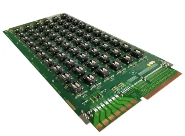
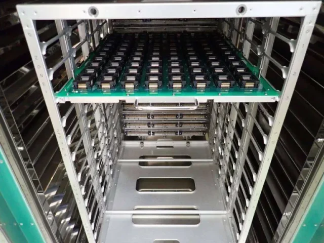
Controlled Test Environment
Using specialized thermal chambers, PCBs are exposed to elevated temperatures and electrical stress patterns under tightly controlled conditions. -
Continuous Monitoring & Data Logging
Real-time data acquisition systems record voltage, current, and temperature parameters to detect any deviations or performance drifts. -
Failure Analysis & Root Cause Identification
Any anomaly triggers immediate analysis. Our reliability engineers trace the issue back to design, process, or component level, ensuring closed-loop quality control.
Benefits of KKPCB’s Burn-in Testing
-
Enhanced Reliability: Early detection of defects ensures stable long-term operation.
-
Improved Product Lifetime: Stress-tested boards maintain consistent electrical performance.
-
Reduced Warranty Risks: Preventing field failures protects both brand reputation and customer trust.
-
Process Validation: Data-driven insights strengthen our overall design-for-reliability (DfR) approach.
Challenges and Industry Considerations
While Burn-in Testing adds time and cost, it ultimately reduces lifecycle expenses by preventing recalls and field failures.
Sensitive components and high-density PCBs require tailored stress profiles to avoid overexposure. KKPCB’s engineering team adjusts parameters per project to balance rigor and safety.
KKPCB’s Commitment to Quality
Our philosophy is simple — every board must perform flawlessly.
Through advanced Burn-in Testing, precision fabrication, and rigorous inspection, KKPCB guarantees that each product meets the highest reliability standards demanded by global OEMs. Whether you need high-frequency RF boards or complex multilayer PCBA assemblies, our processes ensure lasting performance under real-world conditions.
Conclusion
Burn-in Testing is not just a procedure — it’s part of KKPCB’s commitment to reliability, performance, and engineering excellence. By combining scientific precision with advanced manufacturing, KKPCB continues to deliver PCBs that stand the test of time, ensuring our customers’ products operate at their best — always.
