
With the continuous evolution of electronic products toward higher functionality, smaller form factors, and increased signal complexity, traditional single-layer and double-layer PCBs are often unable to meet modern design requirements.
Multilayer PCBs have become an essential technology for advanced electronic systems by providing more routing space, improved electrical performance, and enhanced design flexibility.
By integrating multiple conductive layers with insulating dielectric materials through a laminated structure, multilayer PCBs enable engineers to develop compact and high-performance electronic products used in industries such as:
- Communication equipment
- Automotive electronics
- Industrial control systems
- Medical devices
- Aerospace electronics
- Semiconductor applications
However, designing and manufacturing multilayer PCBs requires careful consideration of stack-up structure, signal integrity, thermal management, material selection, and manufacturing capability.
1. What Is a Multilayer PCB?
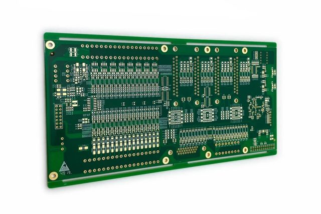
A multilayer PCB is a printed circuit board consisting of three or more conductive copper layers separated by insulating dielectric materials.
Unlike single-layer or double-layer boards, multilayer PCBs contain:
- Outer copper layers
- Inner signal layers
- Power layers
- Ground layers
- Prepreg and core dielectric materials
The layers are bonded together through a lamination process to form a single rigid structure.
A typical multilayer PCB structure may include:
Top Layer → Prepreg → Inner Signal Layer → Core → Power/Ground Layer → Prepreg → Bottom Layer
The exact stack-up depends on:
- Circuit complexity
- Signal requirements
- Mechanical constraints
- Manufacturing capability
2. Why Are Multilayer PCBs Important?
Modern electronic systems require:
- Higher component density
- Faster signal transmission
- Better electromagnetic compatibility
- More efficient power distribution
Multilayer PCBs provide several advantages compared with traditional PCB structures.
2.1 Higher Wiring Density
By adding more copper layers, multilayer PCBs provide additional routing space.
Benefits include:
- Reduced PCB size
- More compact product design
- Support for complex circuits
This is especially important for:
- Smartphones
- Communication modules
- Industrial controllers
2.2 Improved Signal Integrity
High-speed electronic systems require controlled signal transmission.
Dedicated signal layers and reference planes help:
- Reduce interference
- Control impedance
- Minimize signal loss
Multilayer structures are widely used in:
- High-speed digital circuits
- RF systems
- Networking equipment
2.3 Better Power Distribution
Dedicated power and ground planes improve:
- Current distribution
- Voltage stability
- Noise reduction
This is essential for systems with:
- High-speed processors
- Multiple power domains
- Sensitive analog circuits
2.4 Enhanced EMI/EMC Performance
Proper multilayer stack-up design helps control electromagnetic interference.
Ground planes can provide:
- Shielding effects
- Reduced radiation
- Better return current paths
This improves compliance with EMC requirements.
3. Common Types of Multilayer PCBs
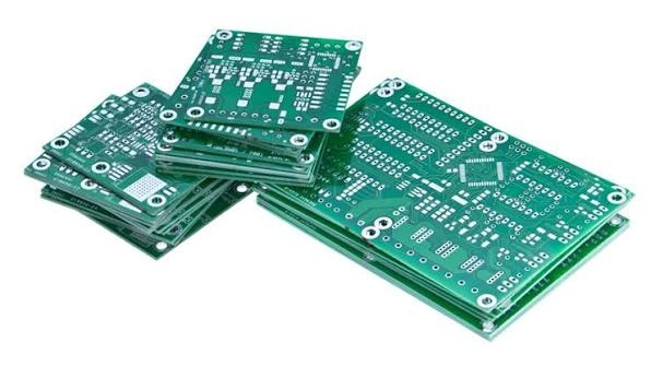
Multilayer PCBs can be categorized based on layer count and structure.
3.1 Standard Multilayer PCB
Common layer counts include:
- 4-layer PCB
- 6-layer PCB
- 8-layer PCB
- 10-layer PCB
- Higher-layer-count PCB
Applications include:
- Industrial equipment
- Control systems
- Communication devices
3.2 HDI Multilayer PCB
High Density Interconnect (HDI) PCBs use advanced structures such as:
- Microvias
- Blind vias
- Buried vias
- Fine-line routing
Advantages include:
- Higher wiring density
- Smaller form factor
- Improved electrical performance
Applications include:
- Mobile devices
- Medical electronics
- High-performance systems
3.3 Rigid-Flex Multilayer PCB
Rigid-flex PCBs combine rigid and flexible materials.
They provide:
- Space-saving design
- Mechanical flexibility
- Improved reliability in moving applications
Common applications:
- Wearable devices
- Aerospace systems
- Medical equipment
4. Multilayer PCB Manufacturing Process
Manufacturing multilayer PCBs requires precise process control.
4.1 Inner Layer Fabrication
The process begins with manufacturing inner copper layers.
Main steps include:
- Copper surface preparation
- Photoresist coating
- Circuit imaging
- Etching
- Inspection
The accuracy of inner layers directly affects final layer alignment.
4.2 Layer Stacking and Lamination
Multiple layers are stacked together with dielectric materials.
The lamination process applies:
- Heat
- Pressure
- Controlled time cycles
to bond all layers into one structure.
Important factors include:
- Temperature control
- Material compatibility
- Layer registration accuracy
4.3 Drilling Process
After lamination, holes are drilled for:
- Through-hole vias
- Component mounting
- Interlayer connections
Advanced multilayer PCBs may require:
- Laser drilling
- Microvia formation
4.4 Copper Plating
The drilled holes are plated with copper to create electrical connections between layers.
The plating process affects:
- Via reliability
- Current capacity
- Signal performance
4.5 Outer Layer Processing
The outer circuit layers are formed through:
- Imaging
- Etching
- Surface treatment
Common surface finishes include:
- ENIG
- ENEPIG
- HASL
- OSP
4.6 Inspection and Testing
Multilayer PCBs require strict quality verification.
Common tests include:
- AOI inspection
- Electrical testing
- Impedance testing
- X-ray inspection
- Cross-section analysis
5. Key Design Considerations for Multilayer PCBs
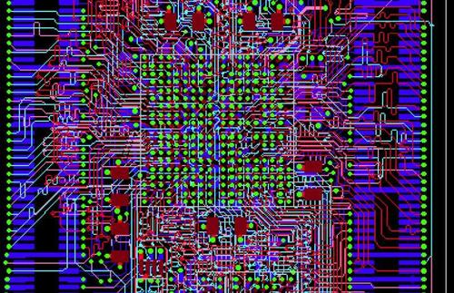
Successful multilayer PCB design requires careful planning.
5.1 Stack-Up Design
The stack-up determines:
- Signal performance
- Power integrity
- Mechanical stability
Engineers should consider:
- Number of layers
- Signal layer arrangement
- Ground plane location
- Dielectric thickness
A well-designed stack-up helps optimize electrical performance and manufacturing reliability.
5.2 Signal Integrity Management
High-speed signals are sensitive to PCB structure.
Important considerations include:
- Controlled impedance
- Differential pair routing
- Length matching
- Reference plane continuity
Poor design may cause:
- Signal reflection
- Crosstalk
- Transmission loss
5.3 Power Integrity Design
Power distribution networks should be carefully optimized.
Recommended practices include:
- Dedicated power planes
- Short power return paths
- Proper decoupling capacitor placement
This helps maintain stable voltage supply.
5.4 Thermal Management
Higher component density increases heat generation.
Thermal solutions may include:
- Larger copper areas
- Thermal vias
- Optimized component placement
5.5 Manufacturing Capability
Design rules should match fabrication capabilities.
Important parameters include:
- Minimum trace width
- Minimum spacing
- Via dimensions
- Layer registration tolerance
Early DFM review helps prevent manufacturing issues.
6. Common Challenges in Multilayer PCB Manufacturing
6.1 Layer Alignment
Misalignment between layers can cause:
- Open circuits
- Reduced annular rings
- Via reliability issues
Precise lamination and registration control are essential.
6.2 PCB Warpage
Multilayer structures may experience warpage due to:
- Uneven copper distribution
- Material differences
- Thermal stress
Proper stack-up design helps reduce deformation.
6.3 Signal Performance Variation
Changes in:
- Material thickness
- Dielectric properties
- Manufacturing tolerance
may affect impedance and signal quality.
7. Applications of Multilayer PCBs
Communication Equipment
Used in:
- Network devices
- RF systems
- Wireless communication equipment
Requirements:
- High-speed transmission
- Controlled impedance
- EMI control
Automotive Electronics
Applications include:
- ADAS systems
- Vehicle control modules
- Battery management systems
Requirements:
- Reliability
- Thermal stability
- Environmental resistance
Industrial Control Systems
Multilayer PCBs support:
- Automation equipment
- PLC systems
- Power control units
Medical Electronics
Applications require:
- High reliability
- Signal accuracy
- Compact design
Conclusion
Multilayer PCBs are a key technology enabling modern electronic products with higher performance, smaller size, and greater functionality.
From stack-up design and signal integrity management to manufacturing precision and reliability testing, every stage influences the final PCB performance.
As electronic systems continue advancing toward higher speed, greater integration, and more demanding environments, multilayer PCB technology will remain essential for future electronic innovation.
By combining optimized design practices with advanced manufacturing capabilities, engineers can achieve reliable, high-performance PCB solutions for a wide range of applications.
