
As semiconductor devices continue to evolve toward higher processing performance, smaller package sizes, and greater integration density, traditional PCB technologies alone are no longer sufficient to meet the interconnection requirements between silicon chips and electronic systems.
IC substrates serve as a critical connection platform between semiconductor chips and printed circuit boards (PCBs), enabling reliable electrical transmission, mechanical support, and thermal management.
They play an essential role in advanced electronic applications including:
- High-performance computing
- Artificial intelligence processors
- Mobile devices
- Automotive electronics
- Semiconductor testing systems
- Communication equipment
Compared with conventional PCBs, IC substrates require much finer line widths, higher interconnection density, and stricter manufacturing control.
This article provides a comprehensive overview of IC substrates, including their structure, types, manufacturing processes, design considerations, and applications.
1. What Is an IC Substrate?
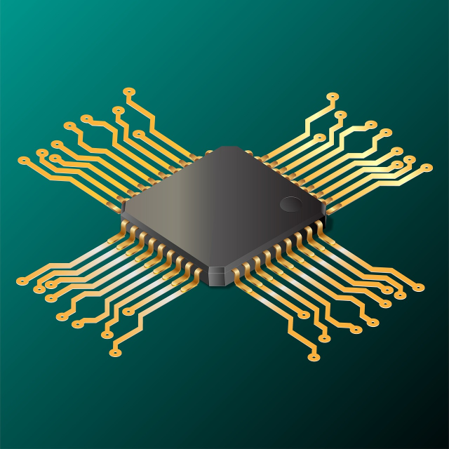
An IC substrate (Integrated Circuit Substrate) is a specialized interconnection board located between a semiconductor chip and a PCB.
Its primary functions are:
- Providing electrical connections between chip and PCB
- Supporting semiconductor packaging
- Distributing power and signals
- Improving mechanical reliability
- Assisting thermal management
The typical connection structure is:
IC Chip → IC Substrate → PCB → Electronic System
The IC substrate acts as an intermediate layer that converts the extremely fine connection points of a semiconductor chip into a larger pitch suitable for PCB assembly.
2. Why IC Substrates Are Important
2.1 Bridging the Gap Between Chip and PCB
Semiconductor chips contain thousands of tiny connection points.
However, conventional PCBs cannot directly connect to these ultra-fine structures.
IC substrates solve this challenge by providing:
- Fine-pitch interconnections
- High-density routing
- Reliable electrical transition
2.2 Supporting Advanced Semiconductor Packaging
As semiconductor technology advances, chip packages require:
- Higher input/output (I/O) density
- Faster signal transmission
- Lower power loss
IC substrates enable advanced packaging technologies such as:
- Flip-chip packaging
- Ball Grid Array (BGA)
- Chip Scale Package (CSP)
- System-in-Package (SiP)
2.3 Improving Electrical Performance
High-speed semiconductor devices require excellent signal integrity.
IC substrates help optimize:
- Signal transmission paths
- Power distribution
- Ground return structures
This reduces:
- Signal loss
- Crosstalk
- Power noise
3. Basic Structure of IC Substrates
An IC substrate typically consists of multiple layers, including:
3.1 Dielectric Layers
Dielectric materials provide:
- Electrical insulation
- Mechanical support
- Layer separation
Common materials include:
- BT resin (Bismaleimide Triazine)
- ABF (Ajinomoto Build-up Film)
- High-performance epoxy materials
3.2 Copper Circuit Layers
Copper layers provide electrical connections.
They are manufactured with:
- Fine-line patterning
- High precision etching
- Microvia technology
3.3 Microvias
Microvias are small laser-drilled holes used for high-density connections.
Advantages:
- Space-saving
- Short electrical paths
- Higher routing density
3.4 Solder Mask and Surface Finish
The surface layer provides:
- Protection
- Soldering reliability
Common finishes include:
- ENIG
- ENEPIG
4. Types of IC Substrates
Different semiconductor applications require different substrate technologies.
4.1 FC-BGA Substrate (Flip-Chip Ball Grid Array)
FC-BGA substrates are widely used for high-performance semiconductor packages.
Characteristics:
- High I/O density
- Excellent signal performance
- Support for large chips
Applications:
- CPUs
- GPUs
- AI processors
- Network processors
4.2 FC-CSP Substrate (Flip-Chip Chip Scale Package)
FC-CSP substrates are designed for compact semiconductor packages.
Advantages:
- Small size
- Lightweight structure
- High integration density
Applications:
- Mobile processors
- Wireless chips
- Consumer electronics
4.3 SiP Substrate (System-in-Package)
SiP substrates integrate multiple semiconductor components into one package.
They support:
- Multiple chips
- Passive components
- Advanced interconnections
Applications:
- IoT modules
- Wearable devices
- RF systems
4.4 Memory IC Substrate
Memory devices require high-speed data transmission.
Applications include:
- DRAM
- Flash memory
- High-bandwidth memory (HBM)
Requirements:
- Low signal loss
- High reliability
- Fine-pitch routing
4.5 RF IC Substrate
RF substrates are designed for high-frequency semiconductor applications.
Requirements:
- Low dielectric loss
- Stable electrical characteristics
- Controlled impedance
Applications:
- Wireless communication chips
- RF modules
- 5G systems
5. IC Substrate Manufacturing Process
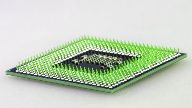
IC substrate manufacturing is highly precise and requires advanced PCB technologies.
5.1 Material Preparation
The process begins with selecting suitable materials based on:
- Electrical requirements
- Thermal performance
- Mechanical reliability
Common materials:
- BT resin
- ABF materials
- High-performance laminates
5.2 Inner Layer Circuit Formation
Circuit patterns are created through:
- Photo imaging
- Copper plating
- Etching
The process requires extremely high precision due to fine-line structures.
5.3 Build-Up Layer Formation
Modern IC substrates use build-up technology.
Process includes:
- Dielectric layer coating
- Laser microvia drilling
- Copper plating
- Circuit pattern formation
Multiple cycles create high-density interconnections.
5.4 Lamination
Layers are bonded together under controlled:
- Temperature
- Pressure
- Time
Proper lamination prevents:
- Delamination
- Internal stress
- Reliability issues
5.5 Surface Finishing
Surface treatment improves:
- Solderability
- Corrosion resistance
Common finishes:
- ENIG
- ENEPIG
5.6 Inspection and Testing
IC substrates require strict quality control.
Testing includes:
Electrical Testing
Checks:
- Continuity
- Insulation resistance
AOI Inspection
Detects:
- Pattern defects
- Line width variation
X-Ray Inspection
Checks:
- Internal structures
- Hidden defects
6. Key Design Considerations for IC Substrates
6.1 Fine-Line Routing Capability
IC substrates require extremely fine circuits.
Important factors:
- Line width and spacing
- Copper thickness
- Manufacturing tolerance
6.2 Signal Integrity
High-speed chips require careful control of:
- Impedance
- Crosstalk
- Signal delay
Design methods include:
- Optimized routing
- Reference plane control
- Differential pair design
6.3 Power Integrity
Modern chips consume significant power.
IC substrates must provide:
- Stable power delivery
- Low-resistance paths
- Effective decoupling structures
6.4 Thermal Management
High-performance chips generate substantial heat.
Thermal design considerations include:
- Heat spreading structures
- Thermal vias
- Material selection
7. IC Substrate vs PCB
| Feature | IC Substrate | PCB |
|---|---|---|
| Main Function | Chip-to-board connection | System-level connection |
| Line Width | Extremely fine | Larger |
| Density | Very high | Medium to high |
| Manufacturing Difficulty | Very high | Lower |
| Main Applications | Semiconductor packaging | Electronic systems |
| Materials | ABF, BT resin | FR-4, Rogers, metal core |
8. Applications of IC Substrates
8.1 Artificial Intelligence and High-Performance Computing
Applications:
- AI accelerators
- GPUs
- Data center processors
Requirements:
- High-speed transmission
- Large I/O capacity
8.2 Mobile Electronics
Applications:
- Smartphones
- Tablets
- Wearable devices
Requirements:
- Miniaturization
- Low power consumption
8.3 Automotive Electronics
Applications:
- Autonomous driving systems
- Vehicle computing platforms
Requirements:
- High reliability
- Temperature resistance
8.4 Communication Equipment
Applications:
- 5G infrastructure
- Network processors
Requirements:
- High-frequency performance
- Signal integrity
8.5 Semiconductor Testing Equipment
Applications:
- IC test boards
- Advanced semiconductor test systems
Requirements:
- Precise electrical performance
- High-density interfaces
9. Challenges in IC Substrate Development
9.1 Increasing Manufacturing Complexity
As semiconductor packages become more advanced:
- Line widths become smaller
- Layer counts increase
- Process control becomes stricter
9.2 Thermal Reliability
Higher chip performance generates more heat.
Challenges include:
- Material expansion mismatch
- Thermal stress
- Package reliability
9.3 Signal Integrity at Higher Speeds
High-speed interfaces require:
- Low-loss materials
- Precise impedance control
- Advanced simulation
9.4 Cost and Yield Control
IC substrate manufacturing requires:
- Advanced equipment
- High process accuracy
- Strict inspection
Maintaining high yield is a major challenge.
10. Future Development Trends of IC Substrates
Higher Density Interconnection
Future IC substrates will continue moving toward:
- Smaller microvias
- Finer lines
- More build-up layers
Advanced Packaging Integration
Technologies such as:
- Chiplets
- 2.5D packaging
- 3D packaging
will increase demand for advanced substrates.
Improved Thermal Solutions
Future substrates will require:
- Better heat dissipation
- Advanced materials
- New thermal structures
Low-Loss High-Speed Materials
As data rates increase, IC substrates will require:
- Lower dielectric loss
- Better signal integrity
- Higher frequency performance
Conclusion
IC substrates are a critical technology connecting semiconductor chips with electronic systems. They provide essential functions including:
- Electrical interconnection
- Mechanical support
- Signal transmission
- Power distribution
- Thermal management
With the continuous growth of AI computing, 5G communication, automotive electronics, and advanced semiconductor packaging, IC substrates will become increasingly important.
Successful IC substrate development requires precise control of:
- Material selection
- Fine-line fabrication
- Microvia technology
- Signal integrity
- Manufacturing reliability
As semiconductor integration continues advancing, IC substrates will remain a key foundation technology enabling next-generation electronic products.
