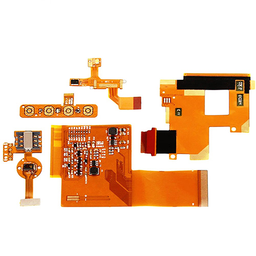
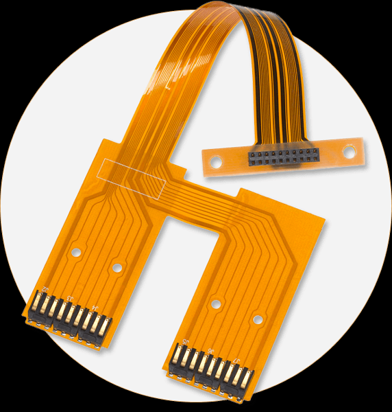
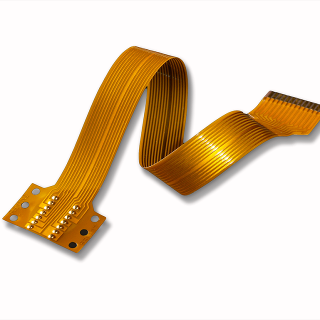
Flexible Printed Circuits (FPCs), commonly known as Flexible PCBs, have revolutionized modern electronics by offering a bendable, lightweight alternative to traditional rigid boards. Made from polyimide (PI) or polyester (PET) base materials, FPCs allow for 3D wiring and high-density packaging, making them indispensable for smartphones, wearables, medical devices, and automotive systems.
Step 1: Material Preparation (Laminate & Cutting)
The process begins with high-quality flexible copper-clad laminates (FCCL). These consist of a thin copper foil bonded to a polyimide film. The material is cut into production panels and pre-baked to remove moisture, ensuring dimensional stability during high-temperature processing.
Step 2: CNC Drilling / Laser Drilling
To create electrical connections between layers (vias), precision drilling is required.
- Mechanical Drilling: Used for larger holes.
- Laser Drilling: Utilized for micro-vias (often as small as 0.05mm) to maintain the high precision required for compact flexible designs.
Step 3: Desmear and Descum (Plasma Cleaning)
Because flexible materials are prone to generating “smear” during drilling, a plasma cleaning process is used. This removes resin debris from the hole walls, ensuring a clean surface for subsequent copper plating.
Step 4: Electroless Copper & VCP Plating
A thin layer of copper is chemically deposited onto the hole walls (electroless plating). This is followed by Vertical Continuous Plating (VCP), which uses electrochemistry to thicken the copper layer, ensuring robust conductivity throughout the vias.
Step 5: Circuit Imaging and Etching
A photosensitive dry film (photoresist) is applied to the panel. Using UV light and a high-resolution mask, the circuit pattern is transferred to the film. The board then passes through an etching line where unwanted copper is chemically removed, leaving only the precise circuit traces.
Step 6: Coverlay Lamination
Unlike rigid PCBs that use liquid solder mask, flexible PCBs use a Coverlay. This is a solid layer of polyimide with an adhesive backing. It is aligned and bonded to the circuit under high heat and pressure in a vacuum press, providing superior flexibility and protection against environmental factors.
Step 7: Surface Finish (ENIG, OSP, or Tin)
To protect the exposed copper pads and ensure reliable soldering, a surface finish is applied. ENIG (Electroless Nickel Immersion Gold) is the most common choice for FPCs due to its excellent flat surface and corrosion resistance, which is vital for fine-pitch components.
Step 8: Stiffener Attachment
Flexible boards often require extra support in areas where components are soldered or connectors are inserted. Stiffeners made of FR-4, Stainless Steel, or PI are bonded to specific areas of the FPC using pressure-sensitive or thermally-cured adhesives.
Step 9: Electrical Testing and Final Cutting
Every FPC undergoes rigorous Electrical Testing (Flying Probe or Dedicated Fixture) to check for open or short circuits. Finally, the individual circuits are cut from the production panel using Laser Cutting or steel dies to ensure smooth, burr-free edges.
