
With the increasing demand for higher efficiency and power density in modern power electronics, superjunction MOSFETs have become an important semiconductor technology for applications such as:
- AC-DC power supplies
- Electric vehicle charging systems
- Industrial power converters
- Renewable energy equipment
- Motor drive systems
- High-efficiency switching regulators
Compared with traditional MOSFET structures, superjunction MOSFETs achieve lower conduction losses and improved switching performance by optimizing the internal electric field distribution.
However, the full performance potential of a superjunction MOSFET does not depend only on the semiconductor device itself. PCB design plays a critical role in determining switching efficiency, thermal performance, EMI behavior, and long-term reliability.
Poor PCB layout may introduce:
- Excessive parasitic inductance
- Switching voltage overshoot
- Increased electromagnetic interference
- Additional switching losses
- Thermal stress
Therefore, optimizing PCB design is essential to maximize the advantages of superjunction MOSFET technology.
1. Understanding Superjunction MOSFET Characteristics
A superjunction MOSFET improves voltage blocking capability by using a multi-column structure inside the semiconductor.
Compared with conventional MOSFETs, it provides:
Lower RDS(on)
The optimized structure reduces conduction resistance.
Benefits:
- Lower conduction loss
- Higher efficiency
- Reduced heat generation
Faster Switching Capability
Superjunction MOSFETs typically support high-frequency switching.
Advantages:
- Smaller magnetic components
- Higher power density
- Improved system efficiency
Higher Voltage Capability
They are commonly used in:
- 600V
- 650V
- 800V
power conversion applications.
However, higher switching speed also increases sensitivity to PCB parasitic effects.
2. Importance of PCB Layout Optimization
The PCB is not simply a connection platform. In high-speed power switching circuits, PCB traces behave as electrical components with:
- Resistance
- Inductance
- Capacitance
Unoptimized PCB design can negatively affect MOSFET performance.
Key PCB design goals include:
- Minimizing switching loop inductance
- Improving heat dissipation
- Controlling EMI
- Ensuring reliable gate driving
3. Minimize High-Current Loop Area
3.1 Switching Loop Optimization
The switching loop includes components such as:
- Superjunction MOSFET
- Diode or synchronous MOSFET
- Input capacitor
- Transformer or inductor
During switching operation, high-frequency current flows through this loop.
A large loop area increases:
- Parasitic inductance
- Voltage overshoot
- EMI radiation
Design Recommendations
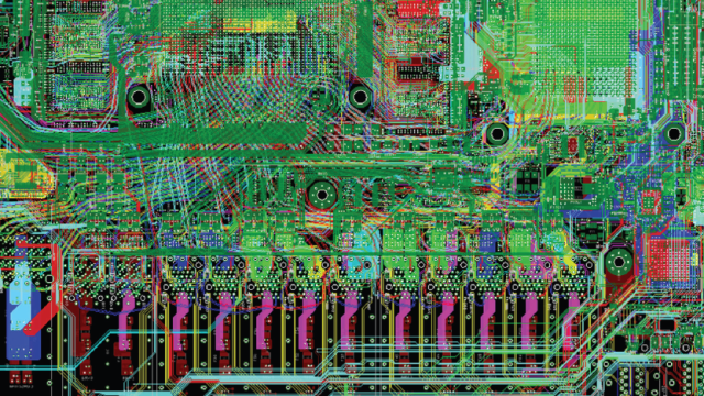
To minimize loop inductance:
- Place input capacitors close to MOSFET terminals
- Keep high-current paths short and wide
- Reduce unnecessary routing layers
- Avoid long return paths
A compact current loop improves:
- Switching efficiency
- Device reliability
- Electromagnetic performance
4. Optimize Gate Drive Circuit Layout
The gate drive circuit directly affects MOSFET switching behavior.
Important parameters include:
- Gate voltage stability
- Switching speed
- Turn-on and turn-off timing
4.1 Keep Gate Loop Short
The gate loop consists of:
- Gate driver output
- Gate resistor
- MOSFET gate terminal
- Source return path
A long gate loop increases:
- Parasitic inductance
- Gate ringing
- Switching noise
Recommended practices:
- Place the gate driver close to the MOSFET
- Minimize gate trace length
- Use direct return paths
4.2 Separate Power and Signal Ground
For high-performance power circuits:
Avoid sharing:
- Gate driver ground
- Control circuit ground
- High-current power return paths
A better approach:
- Use dedicated return paths
- Apply proper grounding strategy
This prevents switching noise from affecting control signals.
5. Control Parasitic Inductance
Parasitic inductance is one of the biggest challenges in high-speed MOSFET applications.
It can cause:
- Voltage spikes
- Ringing
- Additional losses
- Device stress
5.1 Reduce Trace Inductance
Methods include:
- Increasing copper width
- Using thicker copper layers
- Shortening conductor length
- Using multiple parallel vias
5.2 Optimize Via Design
Vias introduce additional inductance.
For high-current paths:
Recommended approaches:
- Use multiple vias
- Avoid small single vias
- Minimize via transition distance
Applications:
- MOSFET source connections
- Power ground connections
6. Improve Thermal Management
Although superjunction MOSFETs have low conduction losses, high switching frequency can still generate significant heat.
PCB thermal design affects:
- Junction temperature
- Efficiency
- Reliability
6.1 Increase Copper Area
Large copper areas improve:
- Heat spreading
- Current distribution
Recommended areas:
- Drain connection
- Source connection
- Power return paths
6.2 Use Thermal Vias
Thermal vias help transfer heat between PCB layers.
Benefits:
- Improved heat dissipation
- Reduced thermal resistance
Common approaches:
- Via arrays under thermal pads
- Connected copper planes
6.3 Select Appropriate PCB Materials
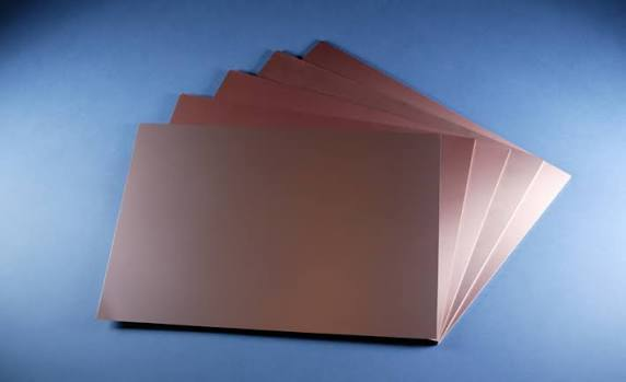
For high-power applications, material selection should consider:
- Thermal conductivity
- Glass transition temperature
- Mechanical reliability
Possible options:
- High-Tg FR-4
- Heavy copper PCB
- Metal core PCB (MCPCB)
7. Optimize EMI Performance
Fast switching characteristics can create electromagnetic interference.
Main sources include:
- High di/dt current loops
- High dv/dt switching nodes
- Gate ringing
PCB EMI Reduction Methods
Reduce Switching Node Area
The drain switching node has high voltage variation.
Recommendations:
- Keep copper area controlled
- Avoid unnecessary routing near sensitive circuits
Add Ground Shielding
Methods:
- Ground planes
- Guard traces
- Shielding structures
Improve Return Path Design
A continuous return path reduces:
- Current loop area
- EMI radiation
8. Select Proper PCB Stack-Up
For multilayer power PCBs, stack-up design is important.
A suitable structure may include:
- Dedicated power layers
- Ground reference planes
- Short current paths
Advantages:
- Lower impedance
- Better thermal performance
- Improved EMI control
9. PCB Design Considerations for Different Applications
AC-DC Power Supplies
Key requirements:
- High voltage isolation
- Low switching loss
- EMI compliance
Important PCB considerations:
- Creepage distance
- Clearance requirements
- Thermal management
EV Chargers
Requirements:
- High efficiency
- High power density
- Long lifetime
PCB priorities:
- Heavy copper design
- Thermal optimization
- Reliable insulation
Industrial Power Converters
Requirements:
- Continuous operation
- High reliability
Design focus:
- Mechanical stability
- Heat dissipation
- Noise control
10. Common PCB Design Mistakes for Superjunction MOSFET Applications
10.1 Long Drain Switching Paths
Problem:
Large switching loop area.
Result:
- Higher EMI
- Increased voltage spikes
10.2 Poor Gate Routing
Problem:
Long gate traces.
Result:
- Gate oscillation
- Unstable switching
10.3 Insufficient Thermal Design
Problem:
Limited copper area.
Result:
- Increased junction temperature
- Reduced lifetime
10.4 Ignoring Parasitic Effects
Problem:
Only considering schematic performance.
Result:
Actual efficiency lower than expected.
11. Verification and Testing
After PCB optimization, engineers should verify performance through:
Electrical Testing
Including:
- Switching waveform measurement
- Voltage overshoot analysis
- Gate signal evaluation
Thermal Testing
Methods:
- Thermal imaging
- Temperature measurement
- Power cycling tests
EMI Testing
Evaluation:
- Conducted emissions
- Radiated emissions
Conclusion
Superjunction MOSFETs provide excellent switching efficiency and power density, but their performance depends heavily on PCB design quality.
To maximize MOSFET performance, engineers should focus on:
- Minimizing switching loop inductance
- Optimizing gate drive layout
- Improving thermal management
- Controlling EMI
- Designing appropriate PCB stack-ups
A well-designed PCB allows superjunction MOSFETs to operate closer to their electrical limits while achieving higher efficiency, improved reliability, and better overall system performance.
