
As electronic products continue evolving toward higher integration, faster signal transmission, and more compact designs, PCB stack-up design has become a critical factor affecting electrical performance and manufacturing reliability.
A PCB stack-up is not simply an arrangement of copper layers and dielectric materials. It determines:
- Signal integrity
- Power distribution performance
- Electromagnetic compatibility (EMC)
- Mechanical stability
- Manufacturing yield
Among various stack-up design strategies, a balanced PCB stack-up is one of the most important approaches for improving board reliability.
An unbalanced PCB structure may lead to:
- Board warpage
- Layer stress imbalance
- Signal integrity issues
- Manufacturing difficulties
A properly balanced stack-up helps achieve better mechanical stability while supporting high-speed and high-density PCB requirements.
1. What Is a Balanced PCB Stack-Up?
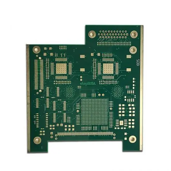
A balanced PCB stack-up refers to a multilayer PCB structure where the materials, copper distribution, and dielectric thickness are arranged symmetrically around the central core layer.
The goal is to maintain mechanical and thermal balance during:
- Lamination
- Drilling
- Soldering
- Assembly processes
A balanced stack-up usually considers:
- Equal or similar copper thickness distribution
- Symmetrical dielectric layer arrangement
- Consistent material properties
- Balanced layer construction
2. Why Is Balanced Stack-Up Design Important?
2.1 Reducing PCB Warpage
During PCB manufacturing, different materials expand and contract at different rates due to temperature changes.
Factors affecting warpage include:
- Copper distribution
- Resin content
- Dielectric thickness
- Lamination temperature
An unbalanced stack-up may create uneven mechanical stress, causing:
- Board bending
- Twisting
- Assembly problems
A symmetrical structure helps distribute stress evenly and improves dimensional stability.
2.2 Improving Manufacturing Reliability
Balanced PCB structures provide better control during manufacturing processes.
Benefits include:
- More stable lamination
- Better layer registration
- Reduced production variation
This is especially important for:
- High-layer-count PCBs
- HDI boards
- Fine-pitch assembly products
2.3 Enhancing Signal Integrity
A balanced stack-up supports better high-speed signal performance by providing:
- Stable reference planes
- Controlled impedance
- Shorter return paths
This is critical for applications such as:
- High-speed processors
- Communication equipment
- RF systems
- Semiconductor test boards
3. Basic Principles of Balanced PCB Stack-Up Design
3.1 Symmetrical Layer Arrangement
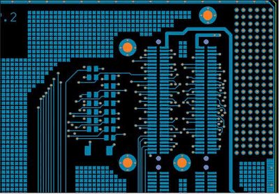
The most fundamental principle is maintaining symmetry around the center of the PCB.
For example:
A 6-layer PCB may be arranged as:
- Layer 1: Signal
- Layer 2: Ground
- Layer 3: Signal/Power
- Core
- Layer 4: Signal/Power
- Layer 5: Ground
- Layer 6: Signal
The upper and lower structures should have similar mechanical characteristics.
3.2 Maintain Copper Balance
Copper distribution significantly affects PCB stress.
Problems may occur when:
- One side contains large copper areas
- The opposite side contains fewer copper areas
Possible results:
- Uneven expansion
- Warpage
- Etching imbalance
Solutions include:
- Adding copper balancing areas
- Optimizing plane distribution
- Adjusting layer assignment
3.3 Keep Dielectric Thickness Balanced
The dielectric thickness between layers affects:
- Mechanical stress
- Impedance performance
- Electrical characteristics
Balanced dielectric structures improve:
- Manufacturing consistency
- Signal predictability
4. Balanced Stack-Up Design for High-Speed PCBs
4.1 Place Reference Planes Properly
High-speed signals require stable reference planes.
Good stack-up design should provide:
- Continuous ground references
- Short return current paths
- Reduced electromagnetic radiation
Common approaches:
- Signal layer adjacent to ground plane
- Dedicated power and ground layers
4.2 Control Impedance Through Stack-Up Design
Impedance depends on:
- Trace width
- Copper thickness
- Dielectric thickness
- Material dielectric constant
A balanced stack-up allows engineers to accurately control:
- Single-ended impedance
- Differential impedance
Common requirements:
- 50Ω single-ended
- 90Ω/100Ω differential
4.3 Optimize Signal Layer Placement
Critical signals should be placed strategically.
Examples:
High-speed signals:
- Close to reference planes
Sensitive RF signals:
- Away from noisy power sections
Power distribution:
- Close to ground layers
5. Balanced Stack-Up Design Methods
5.1 Four-Layer PCB Example
A typical balanced 4-layer structure:
| Layer | Function |
|---|---|
| L1 | Signal |
| L2 | Ground Plane |
| L3 | Power Plane |
| L4 | Signal |
Advantages:
- Simple structure
- Good EMI performance
- Suitable for medium-speed designs
5.2 Six-Layer PCB Example
Example structure:
| Layer | Function |
|---|---|
| L1 | Signal |
| L2 | Ground |
| L3 | Signal |
| L4 | Signal/Power |
| L5 | Ground |
| L6 | Signal |
Advantages:
- Better routing capability
- Improved signal integrity
- Suitable for complex digital systems
5.3 High-Layer PCB Stack-Up
For advanced applications:
- 8-layer
- 10-layer
- 12-layer
- Higher layer count
Design considerations include:
- Symmetrical copper distribution
- Multiple reference planes
- Controlled impedance requirements
Applications:
- Servers
- Industrial control systems
- Communication equipment
6. Material Selection in Balanced Stack-Up Design
6.1 Standard FR-4 Materials
Suitable for:
- General electronic products
- Industrial control boards
Advantages:
- Cost-effective
- Mature manufacturing process
6.2 Low-Loss Materials
For high-frequency applications, engineers may use:
- Low-loss FR-4
- Rogers laminates
- PTFE materials
Benefits:
- Reduced signal loss
- Improved phase stability
- Better high-frequency performance
7. Manufacturing Considerations

7.1 Lamination Control
Lamination affects:
- Layer bonding
- Thickness consistency
- Mechanical stress
Proper control helps maintain stack-up accuracy.
7.2 Layer Registration Accuracy
High-density PCBs require precise alignment.
Poor registration may affect:
- Fine-pitch routing
- Via connection reliability
- Impedance performance
7.3 PCB Thickness Control
Overall thickness variation influences:
- Mechanical stability
- Connector compatibility
- Assembly reliability
8. Common Balanced Stack-Up Design Mistakes
Asymmetric Copper Distribution
Problem:
Different copper density between top and bottom layers.
Impact:
- Warpage
- Mechanical stress
Improper Layer Arrangement
Problem:
Signal layers without proper reference planes.
Impact:
- EMI increase
- Signal degradation
Ignoring Manufacturing Capability
Problem:
Stack-up exceeds fabrication limits.
Impact:
- Lower production yield
- Higher manufacturing cost
Incorrect Material Combination
Problem:
Using unsuitable dielectric materials.
Impact:
- Impedance deviation
- Reliability issues
9. Best Practices for Balanced PCB Stack-Up Design
To achieve a reliable PCB structure:
During Design
- Define electrical requirements first
- Plan layer functions clearly
- Maintain mechanical symmetry
- Consider impedance requirements
During Engineering Review
Evaluate:
- Copper balance
- Material compatibility
- Manufacturing feasibility
- Thermal performance
Before Production
Perform:
- Stack-up verification
- Impedance simulation
- DFM analysis
Conclusion

Balanced PCB stack-up design is a fundamental technique for achieving reliable and high-performance circuit boards.
A properly balanced structure helps:
- Reduce PCB warpage
- Improve manufacturing stability
- Maintain signal integrity
- Support high-speed applications
Successful stack-up design requires careful consideration of:
- Layer arrangement
- Copper distribution
- Dielectric materials
- Impedance requirements
- Manufacturing capability
As PCB technology continues advancing toward higher density and faster signal speeds, balanced stack-up design will remain essential for producing reliable electronic products.
