
In modern PCB assembly, solder paste printing is one of the most critical steps in the SMT manufacturing process.
Before components are placed and soldered, a precise amount of solder paste must be deposited onto specific PCB pads. The quality of this process directly affects:
- solder joint reliability,
- component placement accuracy,
- assembly yield,
- production consistency.
At the center of this process is the PCB stencil — a precision manufacturing tool that controls solder paste volume and placement accuracy.
As electronic products continue moving toward:
- smaller components,
- finer pitch packages,
- higher assembly density,
- more complex PCB layouts,
stencil design and manufacturing have become increasingly important factors in achieving reliable PCBA production.
This article explains the PCB stencil manufacturing process, material selection, cutting technologies, design considerations, and how proper stencil optimization improves SMT assembly quality.
What Is a PCB Stencil?
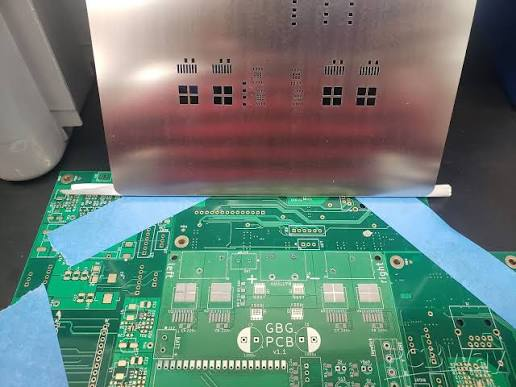
A PCB stencil is a thin metal sheet with precisely created openings (apertures) that match the solder pad locations on a PCB.
During SMT assembly, the stencil is aligned above the PCB, and solder paste is spread across the surface using a squeegee. The paste passes through the stencil openings and is deposited onto the required pads.
After stencil removal, the PCB contains accurately positioned solder paste deposits ready for component placement.
A high-quality stencil ensures:
- consistent solder paste volume,
- accurate pad coverage,
- reduced solder defects,
- improved assembly yield.
Why PCB Stencils Are Important in SMT Assembly
The stencil directly influences the quality of solder paste printing, which affects downstream assembly performance.
1. Solder Paste Printing Accuracy
Incorrect paste volume may cause:
- insufficient solder joints,
- solder bridging,
- component shifting,
- open connections.
Precision stencil manufacturing helps maintain stable solder deposition.
2. Manufacturing Consistency
In high-volume production, manual control is impossible.
A properly designed stencil provides:
- repeatable solder paste printing,
- stable production parameters,
- reduced process variation.
3. Improved Assembly Yield
Many SMT defects originate from poor solder paste printing.
Optimized stencil design helps reduce:
- insufficient solder,
- excessive solder,
- tombstoning,
- solder balls,
- bridging defects.
Common PCB Stencil Materials
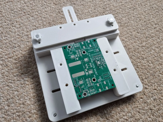
The selection of stencil material affects:
- durability,
- printing accuracy,
- paste release performance,
- production cost.
Common materials include:
| Material | Advantages | Limitations | Applications |
|---|---|---|---|
| Stainless Steel | High durability, excellent precision, cost-effective | Limited flexibility for large formats | Mass production, fine-pitch SMT |
| Nickel | Better flexibility and smooth surface finish | Higher cost | Advanced stencil applications |
| Polyimide (Kapton) | Lightweight and flexible | Shorter lifespan | Prototypes and low-volume production |
| Molybdenum | High strength and dimensional stability | Expensive and less common | High-precision applications |
For most SMT production environments, stainless steel laser-cut stencils are widely used due to their balance of accuracy, durability, and cost.
PCB Stencil Manufacturing Process
The PCB stencil manufacturing process includes several critical stages.
1. Design Data Preparation
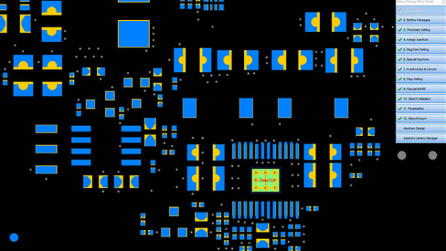
The first step is converting PCB design information into stencil manufacturing data.
Typically, engineers extract:
- solder paste layer data,
- component pad information,
- PCB panel dimensions.
The stencil design is then optimized according to:
- component package type,
- pad geometry,
- solder paste requirements,
- assembly process conditions.
Important design factors include:
- aperture size,
- aperture shape,
- stencil thickness,
- component pitch,
- thermal pad structure.
2. Stencil Material Selection
The appropriate stencil material depends on:
- production volume,
- component density,
- required precision,
- expected stencil lifetime.
For example:
- Prototype assembly → flexible or low-cost stencil solutions
- High-volume SMT production → stainless steel precision stencils
- Fine-pitch BGA/QFN assembly → high-quality laser-cut or electroformed stencils
3. Stencil Cutting Technologies
Several technologies are used to manufacture PCB stencils.
Laser Cutting
Laser cutting is currently the most common stencil manufacturing method.
Advantages:
- high dimensional accuracy,
- suitable for fine-pitch components,
- complex aperture capability,
- no mechanical tool wear.
Typical applications include:
- BGA,
- QFN,
- 0201/01005 components,
- high-density PCB assembly.
Limitations:
- equipment investment cost,
- possible heat influence during cutting.
Chemical Etching
Chemical etching was widely used in earlier stencil production.
Advantages:
- suitable for large stencil formats,
- no thermal impact.
Limitations:
- lower precision,
- less suitable for advanced fine-pitch applications.
Electroforming
Electroformed stencils are produced by growing nickel material layer by layer.
Advantages:
- extremely smooth aperture walls,
- excellent solder paste release,
- suitable for ultra-fine pitch applications.
Limitations:
- higher cost,
- longer manufacturing cycle.
4. Cutting and Manufacturing Process
During laser stencil production, the process includes:
- Loading stainless steel foil into the laser system.
- Importing optimized stencil data.
- Adjusting laser parameters.
- Cutting precise apertures.
- Inspecting dimensional accuracy.
The quality of aperture walls directly affects solder paste release performance.
5. Post-Processing Treatment
After cutting, additional processes may improve stencil performance.
Cleaning
Removes:
- cutting residue,
- metal particles,
- surface contamination.
Methods include:
- ultrasonic cleaning,
- chemical cleaning,
- specialized stencil cleaning processes.
Electropolishing
Electropolishing smooths aperture walls to improve:
- solder paste transfer efficiency,
- paste release,
- printing consistency.
Nano-Coating
Advanced nano-coatings provide:
- lower solder paste adhesion,
- easier cleaning,
- longer stencil lifetime.
Frame Mounting and Tension Control
For framed stencils, the foil must be properly tensioned.
Incorrect tension may cause:
- printing misalignment,
- uneven paste deposition,
- production instability.
PCB Stencil Design Considerations
Stencil manufacturing quality alone is not enough. Proper stencil design is equally important.
1. Aperture Size and Shape Optimization
Aperture design affects solder paste volume.
Common considerations:
- pad dimensions,
- component type,
- solder paste requirements.
Typical adjustments include:
- reducing aperture size for fine-pitch components,
- modifying shapes for thermal pads,
- optimizing openings for BGA and QFN packages.
2. Area Ratio Control
The area ratio is an important indicator of solder paste release performance.
Formula:
Area Ratio = Aperture Area / Aperture Wall Area
General guideline:
| Area Ratio | Paste Release Performance |
|---|---|
| >0.66 | Excellent |
| 0.5–0.66 | Acceptable |
| <0.5 | Higher risk of poor release |
Low area ratios may cause insufficient solder paste transfer.
3. Step Stencils
Step stencils use different thicknesses in different areas.
They are useful when a PCB contains:
- fine-pitch ICs,
- large thermal pads,
- mixed component sizes.
Benefits:
- controlled solder volume,
- reduced solder defects,
- improved assembly reliability.
4. Thermal Pad Design
Large exposed pads, especially for QFN packages, require careful stencil optimization.
Common techniques include:
- windowpane openings,
- segmented apertures,
- home plate designs.
These help reduce:
- solder voids,
- component floating,
- solder ball formation.
Stencil Quality Control
Before production use, stencils should undergo inspection.
Key inspection items include:
- aperture dimensions,
- aperture position accuracy,
- surface quality,
- stencil flatness,
- tension measurement.
Proper inspection helps prevent SMT defects before they reach production.
PCB Stencil Maintenance and Lifecycle Management
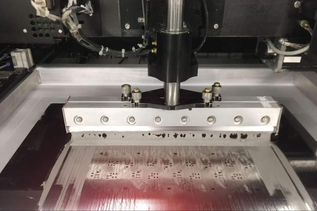
A stencil requires proper maintenance to maintain printing quality.
Cleaning
Recommended practices:
- clean after production cycles,
- remove solder paste residue,
- use suitable cleaning materials.
Storage
Proper storage prevents:
- deformation,
- contamination,
- surface damage.
Recommended conditions:
- dry environment,
- protective packaging,
- dedicated storage racks.
Replacement
Stencils should be replaced when showing:
- dimensional changes,
- damaged apertures,
- reduced printing consistency.
Advanced PCB Stencil Technologies
As PCB assembly continues toward higher density and smaller components, stencil technologies are evolving.
Nano-Coated Stencils
Improve:
- solder paste release,
- cleaning efficiency,
- printing stability.
3D Printed Stencils
Potential advantages:
- rapid prototype manufacturing,
- customized structures.
Current limitations:
- material performance,
- precision control.
Smart Stencils
Future stencil technologies may integrate:
- sensors,
- process monitoring,
- automated inspection functions.
These technologies could enable real-time manufacturing optimization.
Conclusion
PCB stencil manufacturing is a critical part of the SMT assembly process. Although the stencil is only one component of the production workflow, its design and quality directly influence solder paste printing accuracy, assembly yield, and product reliability.
As PCB assemblies become:
- smaller,
- denser,
- more complex,
engineers must pay greater attention to:
- stencil material selection,
- aperture optimization,
- printing process control,
- manufacturing compatibility.
By integrating proper stencil design with DFM analysis and advanced SMT processes, manufacturers can reduce assembly risks and achieve more stable PCB production.
KKPCB supports customers with PCB fabrication, PCBA assembly, and engineering optimization services, helping identify potential manufacturing challenges before production and improving overall product readiness.
