Understanding Ceramic PCB Technology
As modern electronics continue evolving toward higher power density, higher frequency, and improved thermal performance, traditional FR4 PCB materials are no longer sufficient for many advanced applications. This has led to the rapid adoption of Ceramic PCB technology, especially Alumina PCB substrates, in industries requiring:
- Excellent heat dissipation
- High electrical insulation
- High-frequency stability
- Long-term reliability
Ceramic PCBs and ceramic substrates are widely used in:
- Power electronics
- LED lighting systems
- Automotive electronics
- RF and microwave systems
- Aerospace and medical devices
What is a Ceramic PCB?
A Ceramic PCB is a printed circuit board manufactured using a ceramic material as the substrate instead of traditional fiberglass-based FR4 material.
Unlike conventional PCBs, ceramic substrate PCBs provide:
- Extremely high thermal conductivity
- Excellent electrical insulation
- Superior high-temperature resistance
- Stable high-frequency electrical performance
Ceramic PCBs are ideal for:
- High-power electronic systems
- RF and microwave applications
- Harsh industrial environments
What is an Alumina PCB?
An Alumina PCB is the most common type of ceramic PCB, using Aluminum Oxide (Al₂O₃) as the ceramic substrate material.
Alumina PCB Characteristics
- Good thermal conductivity
- Excellent insulation performance
- High mechanical strength
- Cost-effective ceramic material solution
Typical alumina purity:
- 92% Alumina
- 96% Alumina
- 99% Alumina
Higher purity provides:
- Better thermal performance
- Improved electrical characteristics
- Higher manufacturing cost
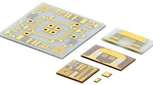
Structure of Ceramic PCB and Alumina PCB
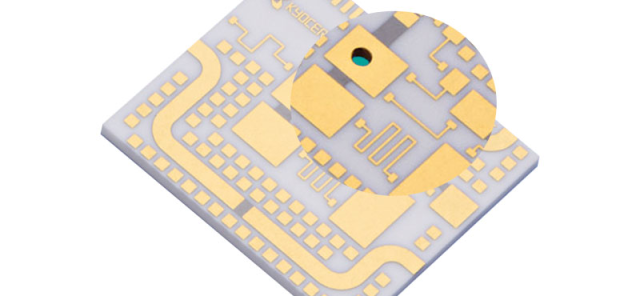
A typical ceramic PCB structure includes:
- Ceramic substrate layer
- Copper conductive layer
- Surface finish layer
- Solder mask or protective coating (optional)
Copper circuits are formed using:
- DBC (Direct Bonded Copper)
- DPC (Direct Plated Copper)
- Thick film or thin film technology
Types of Ceramic PCB Technologies
1. Alumina Ceramic PCB
Most widely used ceramic PCB type.
Advantages:
- Cost-effective
- Good thermal performance
- High reliability
Applications:
- LED modules
- Power supplies
- Industrial electronics
2. Aluminum Nitride (AlN) PCB
Features:
- Extremely high thermal conductivity
- Excellent high-frequency performance
- Superior thermal expansion matching
Applications:
- High-power RF systems
- Automotive power modules
- Semiconductor packaging
3. Beryllium Oxide (BeO) PCB
Features:
- Very high thermal conductivity
- Excellent electrical properties
Limitation:
- Toxic material handling concerns
Used in specialized military and aerospace systems.
Advantages of Ceramic PCB and Alumina PCB
1. Excellent Thermal Conductivity
Ceramic substrates dissipate heat far better than FR4:
- Improved thermal management
- Reduced operating temperature
- Higher power handling capability
Important for:
- Power electronics
- LED PCB applications
- High-power RF systems
2. High Electrical Insulation
Ceramic materials provide:
- Excellent dielectric insulation
- High breakdown voltage
- Stable electrical isolation
Critical for:
- High-voltage systems
- Power modules
- Automotive electronics
3. Superior High-Temperature Resistance
Ceramic PCBs can withstand:
- Extremely high operating temperatures
- Thermal cycling stress
- Harsh industrial environments
4. Excellent High-Frequency Performance
Ceramic PCB materials support:
- Low dielectric loss
- Stable dielectric constant (Dk)
- High-frequency signal transmission
Widely used in:
- RF PCB design
- Microwave circuits
- 5G communication systems
5. Strong Mechanical Stability
Ceramic substrates offer:
- Low thermal expansion
- Excellent dimensional stability
- High mechanical strength
Ceramic PCB Manufacturing Process
1. Ceramic Substrate Preparation
The ceramic material is:
- Sintered at high temperature
- Machined to required thickness and size
2. Copper Circuit Formation
Methods include:
- Direct bonded copper (DBC)
- Direct plated copper (DPC)
- Thick film printing
3. Laser Drilling and Patterning
Precision laser processing enables:
- Fine-line circuit formation
- Microvia processing
- High-density ceramic PCB design
4. Surface Finish Processing
Common finishes:
- ENIG
- Silver plating
- Gold plating
5. Final Inspection and Testing
Includes:
- Electrical testing
- Thermal performance testing
- Reliability validation
Applications of Ceramic PCB and Alumina PCB
1. Power Electronics
- Power converters
- IGBT modules
- Motor drives
2. LED Lighting Systems
- High-power LED PCB modules
- Automotive lighting systems
3. RF and Microwave Systems
- RF amplifiers
- Radar modules
- High-frequency communication systems
4. Automotive Electronics
- EV power systems
- ADAS radar modules
- Battery management systems (BMS)
5. Aerospace and Defense
- Satellite communication systems
- Military radar electronics
- High-reliability avionics
6. Medical Electronics
- Medical imaging systems
- Surgical devices
- High-reliability monitoring equipment
Challenges of Ceramic PCB Manufacturing
1. Higher Manufacturing Cost
Ceramic materials and processes are more expensive than FR4 PCB manufacturing.
2. Brittle Material Characteristics
Ceramic substrates are:
- Hard but brittle
- Sensitive to mechanical shock
3. Complex Manufacturing Process
Requires:
- Precision laser machining
- Advanced metallization technology
- Specialized fabrication equipment
Future Trends in Ceramic PCB Technology
1. High-Power EV Applications
Growing use in:
- Electric vehicle power modules
- Fast charging systems
2. 5G and mmWave RF Systems
Ceramic PCB technology supports:
- High-frequency signal integrity
- Low-loss RF transmission
3. Advanced Semiconductor Packaging
Used in:
- Chip packaging substrates
- AI and high-performance computing systems
4. High Thermal Conductivity Materials
Development of:
- Advanced AlN substrates
- Hybrid ceramic materials
Conclusion
Ceramic PCB and Alumina PCB technologies provide critical advantages in:
- Thermal management
- High-frequency performance
- Electrical insulation
- Long-term reliability
Compared with traditional FR4 PCBs, ceramic substrate PCBs are ideal for:
- High-power electronics
- RF and microwave systems
- Automotive and aerospace applications
- Industrial and medical devices
As electronics continue moving toward higher power density, miniaturization, and high-frequency operation, ceramic PCB technology will play an increasingly important role in next-generation electronic systems.
