
In PCB design, trace thickness and current carrying capacity are closely related factors that directly affect the reliability and performance of electronic systems.
As electronic products continue moving toward higher power density, smaller form factors, and increased functionality, PCB traces must handle higher currents while maintaining acceptable temperature rise and electrical stability.
Insufficient copper thickness or improper trace width design may lead to:
- Excessive temperature rise
- Voltage drop
- Copper trace overheating
- Reduced product lifetime
- Potential circuit failure
Therefore, optimizing the relationship between PCB trace thickness and current capacity is a key consideration in power electronics, automotive systems, industrial equipment, and high-performance electronic products.
1. Understanding PCB Trace Thickness
1.1 What Is PCB Copper Thickness?
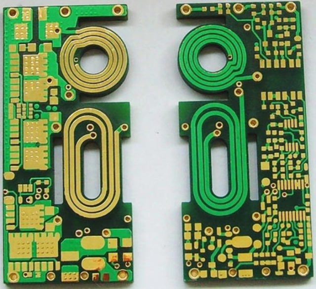
PCB copper thickness refers to the thickness of the copper layer used to form electrical traces on a circuit board.
It is commonly measured in:
- oz (ounce)
- μm (micrometers)
Typical PCB copper thickness options include:
| Copper Thickness | Approximate Thickness |
|---|---|
| 0.5 oz | 17 μm |
| 1 oz | 35 μm |
| 2 oz | 70 μm |
| 3 oz | 105 μm |
| 4 oz | 140 μm |
Standard PCB designs commonly use 1 oz copper, while high-current applications often require thicker copper layers.
2. Relationship Between Copper Thickness and Current Capacity
2.1 Why Does Copper Thickness Affect Current Carrying Capability?
Electrical current flowing through a PCB trace generates heat due to resistance.
The basic relationship is:
Higher current → Higher heat generation
Increasing copper thickness reduces electrical resistance and improves heat dissipation.
A thicker copper layer provides:
- Lower resistance
- Higher current capacity
- Reduced voltage drop
- Better thermal performance
2.2 Current Capacity Depends on Multiple Factors
Copper thickness alone does not determine current capability.
Other important factors include:
- Trace width
- Trace length
- Copper weight
- Temperature rise requirement
- PCB material
- Ambient temperature
- Layer location
For example:
An external layer trace generally dissipates heat better than an internal layer trace because it has better exposure to air.
3. Key Factors Affecting PCB Trace Current Capacity
3.1 Trace Width
Trace width is one of the most important factors affecting current capacity.
A wider trace provides:
- Larger cross-sectional area
- Lower resistance
- Better heat dissipation
Power supply and high-current traces typically require wider routing compared with signal traces.
3.2 Copper Thickness
Increasing copper thickness improves:
- Current handling capability
- Mechanical strength
- Thermal stability
Heavy copper PCBs are commonly used in:
- Power converters
- Battery systems
- Motor control boards
3.3 Allowable Temperature Rise
PCB trace design usually considers acceptable temperature rise.
Excessive temperature may cause:
- Insulation aging
- Material degradation
- Component stress
Engineers typically define maximum temperature rise based on:
- Application environment
- Reliability requirements
- Operating conditions
3.4 PCB Layer Position
The same trace size may have different current capacity depending on its location.
Outer Layer Traces
Advantages:
- Better heat dissipation
- Easier thermal transfer
Inner Layer Traces
Limitations:
- Heat is trapped between dielectric layers
- Lower cooling efficiency
Therefore, inner layer power traces may require larger dimensions.
4. PCB Trace Thickness Optimization Methods
4.1 Select Appropriate Copper Weight
The copper thickness should match the application requirements.
Standard Copper (1 oz–2 oz)
Suitable for:
- Consumer electronics
- Control boards
- Low to medium power applications
Heavy Copper (3 oz or Above)
Suitable for:
- Power electronics
- Battery systems
- High-current circuits
Advantages:
- Higher current capacity
- Improved thermal reliability
4.2 Optimize Trace Width According to Current
During PCB layout design, engineers should calculate:
- Required current
- Maximum temperature rise
- Available board space
Then determine:
- Trace width
- Copper thickness
Avoid designing traces only based on physical space limitations.
4.3 Use Copper Pour and Thermal Reinforcement
For high-current areas, additional copper structures can improve performance.
Methods include:
- Copper pours
- Power planes
- Multiple parallel traces
- Thermal vias
Benefits:
- Reduced resistance
- Improved heat spreading
- Better current distribution
4.4 Use Multiple Layers for High Current Paths
For high-power PCB designs, current can be distributed across multiple layers.
Advantages include:
- Lower current density
- Reduced heating
- Improved reliability
Common applications:
- Power modules
- Inverters
- Battery management systems
5. Heavy Copper PCB Applications
5.1 Power Electronics
Power systems require reliable current transmission.
Applications:
- Power converters
- Switching power supplies
- Motor controllers
Heavy copper improves:
- Thermal performance
- Current capacity
- Long-term stability
5.2 Electric Vehicles
EV systems require PCBs capable of handling high currents.
Applications include:
- Battery management systems
- Charging systems
- Power control modules
PCB copper thickness optimization helps improve:
- Safety
- Reliability
- Thermal management
5.3 Industrial Equipment
Industrial electronics often operate continuously under demanding conditions.
Examples:
- Automation controllers
- Industrial drives
- Power control systems
Heavy copper PCBs provide improved durability.
5.4 LED Lighting Systems
High-power LED systems generate significant heat.
Copper thickness optimization helps:
- Transfer heat efficiently
- Maintain stable brightness
- Extend LED lifetime
6. Common PCB Trace Thickness Design Mistakes
6.1 Using Standard Copper Thickness for High-Current Applications
Problem:
A design uses standard copper without considering actual current requirements.
Possible results:
- Excessive heating
- Voltage instability
- Reduced reliability
6.2 Insufficient Trace Width
Problem:
Trace width is too narrow for the required current.
Results:
- Higher resistance
- Increased temperature rise
6.3 Ignoring Thermal Conditions
Problem:
Only electrical parameters are considered.
However, real applications involve:
- Ambient temperature
- Enclosure conditions
- Cooling methods
6.4 Neglecting Manufacturing Capability
Heavy copper PCB production requires attention to:
- Etching accuracy
- Layer registration
- Copper balance
Improper design may affect:
- Production yield
- Cost
- Reliability
7. Manufacturing Considerations for Thick Copper PCB
7.1 Copper Etching Control
Thicker copper requires careful process control.
Challenges include:
- Line width variation
- Undercutting
- Fine feature limitations
7.2 Via Reliability
High-current designs require proper via selection.
Considerations include:
- Via diameter
- Copper plating thickness
- Thermal stress
Heavy copper vias improve current transfer between layers.
7.3 Thermal Stress Management
Different copper thickness areas may create uneven thermal expansion.
Design optimization helps reduce:
- Warpage
- Mechanical stress
- Reliability issues
8. How Engineers Optimize PCB Current Capacity
A complete optimization process includes:
Step 1: Analyze Electrical Requirements
Evaluate:
- Maximum operating current
- Peak current conditions
- Voltage drop limitations
Step 2: Select PCB Structure
Determine:
- Copper thickness
- Layer count
- Power plane arrangement
Step 3: Perform Thermal Evaluation
Analyze:
- Heat generation
- Temperature rise
- Cooling conditions
Step 4: Validate Manufacturing Feasibility
Review:
- PCB fabrication capability
- Copper balance
- Assembly requirements
Conclusion
Optimizing PCB trace thickness and current capacity is essential for designing reliable electronic systems, especially in high-power and high-reliability applications.
A successful PCB current design requires balancing:
- Copper thickness
- Trace width
- Thermal performance
- Electrical requirements
- Manufacturing capability
By selecting the appropriate copper weight, optimizing trace geometry, and applying proper thermal management strategies, engineers can improve PCB reliability, reduce failure risks, and ensure stable operation in demanding electronic applications.
