What Is Ball Grid Array (BGA) Technology?
Ball Grid Array (BGA) is an advanced surface mount packaging technology widely used in modern electronic products requiring high pin counts, high-speed signal transmission, and compact PCB layouts. Unlike traditional leaded packages, BGA components use an array of solder balls located underneath the package to create electrical and mechanical connections with the PCB.
With the rapid development of high-performance computing, 5G communication, AI hardware, automotive electronics, and industrial control systems, BGA technology has become a core solution for achieving high-density PCB assembly and high-speed electronic design.
What Is a Ball Grid Array (BGA)?
A Ball Grid Array package is an integrated circuit package that uses:
- Solder balls instead of leads
- Bottom-side array connection structure
- Surface mount assembly process
The solder balls provide:
- Electrical interconnection
- Mechanical support
- Thermal conduction paths
Compared with traditional packages such as QFP, BGA technology offers:
- Higher I/O density
- Better electrical performance
- Improved heat dissipation
- Smaller package size
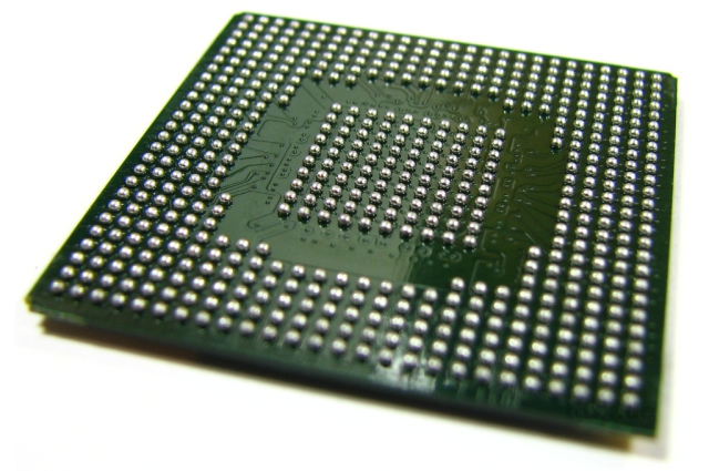
Structure of a Ball Grid Array Package
A typical BGA package structure includes:
- Silicon die
- Substrate layer
- Bond wires or flip-chip interconnects
- Solder mask layer
- Solder ball array
The BGA solder ball array is arranged in a grid pattern to maximize connection density.
Types of Ball Grid Array Packages
1. Plastic Ball Grid Array (PBGA)
Features:
- Cost-effective packaging solution
- Plastic substrate structure
- Widely used in consumer electronics
Applications:
- Motherboards
- Communication modules
- Industrial electronics
2. Ceramic Ball Grid Array (CBGA)
Features:
- Ceramic substrate for better thermal performance
- High reliability
- Excellent dimensional stability
Applications:
- Aerospace electronics
- Military electronics
- High-reliability systems
3. Tape Ball Grid Array (TBGA)
Features:
- Flexible tape substrate
- Lightweight structure
- Good thermal characteristics
Applications:
- Portable electronics
- Compact devices
4. Micro BGA (µBGA)
Features:
- Extremely small package size
- Ultra-high-density interconnection
- Fine-pitch solder ball design
Applications:
- Smartphones
- Wearable electronics
- Miniaturized devices
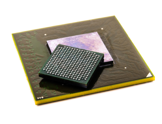
5. Flip-Chip BGA (FCBGA)
Features:
- Direct chip-to-substrate interconnection
- Very high electrical performance
- Excellent signal integrity
Applications:
- CPUs and GPUs
- AI processors
- High-speed computing systems
Advantages of Ball Grid Array Technology
1. High Interconnection Density
BGA supports:
- Large pin counts
- Compact PCB layout
- Smaller package footprint
Essential for:
- HDI PCB design
- Advanced computing systems
2. Improved Electrical Performance
Shorter interconnect paths reduce:
- Signal inductance
- Noise and crosstalk
- Signal delay
This improves:
- Signal integrity
- High-speed data transmission
- RF performance
3. Better Thermal Dissipation
The solder ball array improves:
- Heat transfer efficiency
- Thermal conductivity
- Power handling capability
Important for:
- High-power ICs
- High-speed processors
4. Enhanced Mechanical Reliability
Compared with leaded packages:
- Reduced lead damage risk
- Better vibration resistance
- Stronger solder joint structure
BGA PCB Design Considerations
1. PCB Layer Stack-Up Design
BGA routing often requires:
- Multilayer PCB structures
- Dedicated power and ground planes
- Controlled impedance routing
2. Via Design for BGA
Common solutions:
- Via-in-pad technology
- Blind and buried vias
- Microvia structures
Proper via design improves:
- Routing density
- Signal integrity
- PCB manufacturability
3. Thermal Management
High-power BGA devices require:
- Thermal vias
- Copper planes
- Heat sinks
4. Fine-Pitch Routing
Advanced BGA packages need:
- Fine trace width and spacing
- High-precision PCB manufacturing
- HDI PCB fabrication technology
BGA Assembly Process
1. Solder Paste Printing
High-precision stencil printing is critical for:
- Accurate solder volume
- Fine-pitch alignment
2. Pick-and-Place Assembly
Automated SMT machines place:
- BGA components with micron-level accuracy
3. Reflow Soldering
Controlled thermal profile ensures:
- Proper solder ball collapse
- Reliable solder joints
4. Inspection and Testing
Since solder joints are hidden:
- X-ray inspection is required
- AOI alone is insufficient
Common inspection methods:
- X-ray analysis
- ICT testing
- Functional testing
Common BGA Soldering Defects
1. BGA Solder Bridging
Cause:
- Excess solder paste
- Misalignment
2. Voiding
Cause:
- Gas entrapment during reflow
Effect:
- Reduced thermal performance
3. Head-in-Pillow Defect
Cause:
- Poor solder ball wetting
- Warpage during reflow
4. Cold Solder Joints
Cause:
- Improper reflow profile
- Oxidized solder balls
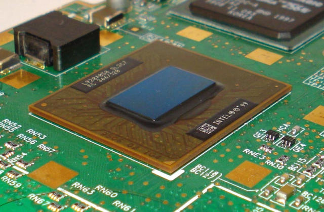
Applications of Ball Grid Array Technology
- CPUs and GPUs
- AI and edge computing systems
- Automotive electronics
- 5G communication equipment
- Aerospace and defense systems
- Medical electronics
- High-speed networking hardware
Future Trends in BGA Technology
1. Higher Pin Density
Advanced packaging supports:
- More I/O connections
- Smaller package sizes
2. AI and High-Performance Computing
FCBGA technology is critical for:
- AI accelerators
- Data center processors
3. Advanced HDI PCB Integration
Supports:
- Smaller form factors
- Faster signal transmission
4. Improved Thermal Packaging
Future BGA designs focus on:
- Advanced heat dissipation
- High-power device reliability
Conclusion
Ball Grid Array (BGA) technology is one of the most important advanced electronic packaging technologies in modern PCB assembly. By providing:
- High-density interconnection
- Excellent signal integrity
- Improved thermal performance
- Compact package design
BGA technology enables the development of modern:
- High-speed computing systems
- AI hardware
- 5G communication devices
- Automotive electronics
- Industrial automation equipment
As electronics continue moving toward higher performance and miniaturization, BGA packaging technology will remain a core solution in advanced PCB design and assembly manufacturing.
