
This article explains how an OBC is structured, which PCB technologies each stage needs, and what to check when choosing materials, copper weights and spacing. Manufacturing values come from KKPCB’s published PCB capabilities.
1. What Does an On-Board Charger Do?
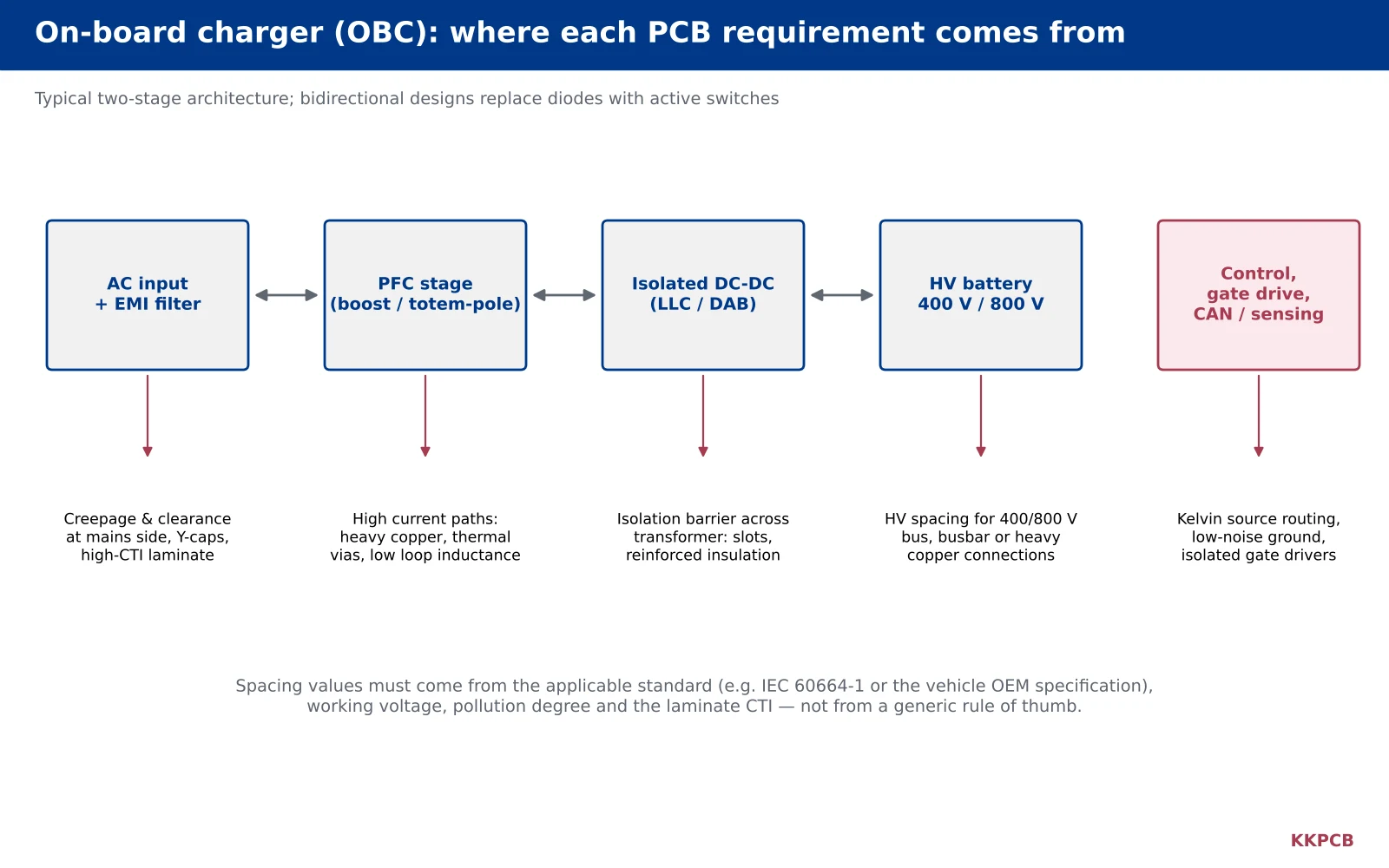
Most OBCs use a two-stage architecture:
- AC input and EMI filter – connects to the charging inlet and keeps conducted noise within limits.
- Power factor correction (PFC) – converts AC to a regulated DC link, often with a boost or totem-pole topology.
- Isolated DC-DC converter – typically an LLC resonant or dual-active-bridge (DAB) stage that provides galvanic isolation and adjusts to the battery voltage.
- Control, gate drive and communication – microcontroller, isolated gate drivers, current and voltage sensing and vehicle CAN communication.
OBCs are commonly rated at power levels such as 3.3, 6.6, 11 or 22 kW. Many newer designs use silicon carbide (SiC) or gallium nitride (GaN) switches for higher efficiency and power density, which raises switching speeds and makes PCB layout even more important.
2. On-Board Charger PCB Requirements Stage by Stage
| OBC stage | Main PCB challenge | Typical PCB response |
|---|---|---|
| AC input / EMI filter | Mains voltage spacing, Y-capacitor placement, surge paths | Creepage and clearance to the applicable standard, high-CTI laminate, slots where needed |
| PFC stage | High RMS current, switching heat, fast edges | Heavy copper, thermal vias under power devices, compact switching loops |
| Isolated DC-DC | Isolation barrier across the transformer, resonant currents | Reinforced insulation design, clear isolation zones, controlled internal layer spacing |
| HV battery output | 400 V / 800 V DC bus, high current | Wide spacing, heavy copper or busbar connections, current-sense layout |
| Control and gate drive | Noise immunity, isolated drivers, sensing accuracy | Kelvin source routing, low-inductance gate loops, quiet ground reference |
3. Heavy Copper for High-Current Paths
Current capacity is limited by copper cross-section and the allowable temperature rise. In an OBC, the PFC inductor current, DC-link connections and output paths often need far more copper than a standard 1 oz layer can provide. Heavy copper layers reduce resistance and spread heat away from the power devices.
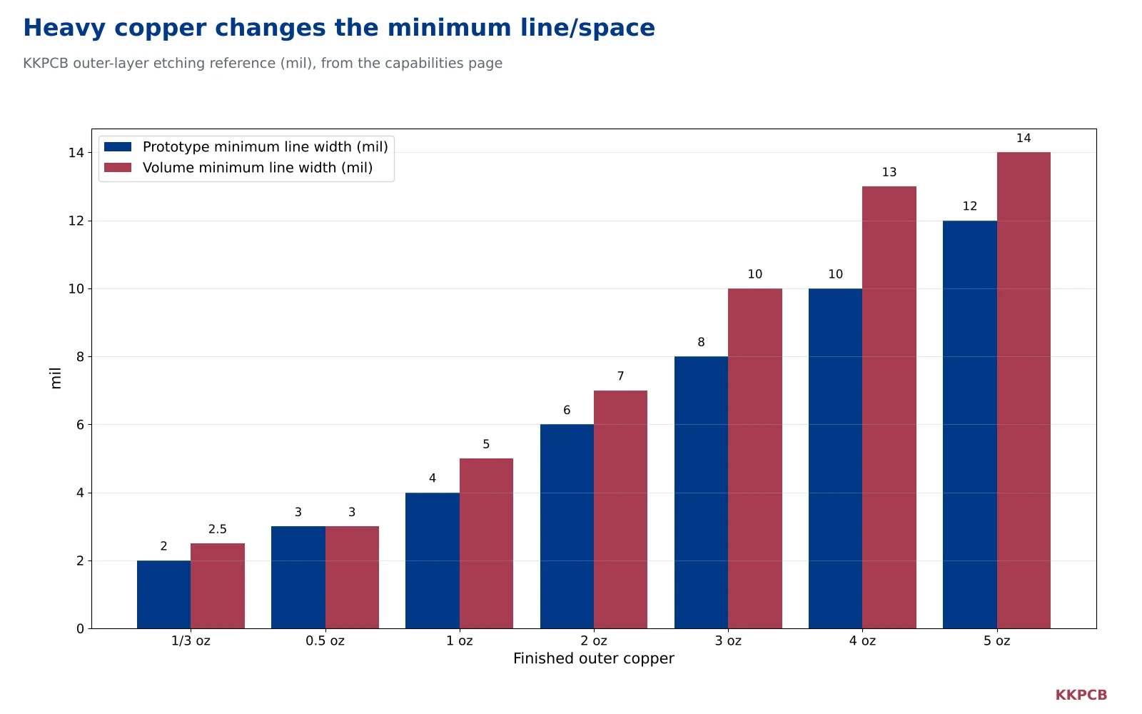
KKPCB builds finished copper up to 14 oz on outer layers and 12 oz on inner layers. Heavy copper changes the rules for fine features, because thicker copper needs wider spacing to etch reliably:
| Outer-layer copper | Minimum line / space (prototype, mil) | Minimum line / space (volume, mil) |
|---|---|---|
| 1 oz | 4 / 4 | 5 / 5 |
| 2 oz | 6 / 6 | 7 / 7 |
| 3 oz | 8 / 8 | 10 / 10 |
| 4 oz | 10 / 13 | 13 / 13 |
| 5 oz | 12 / 15 | 14 / 14 |
A common strategy is to place heavy copper on inner power layers and keep moderate copper on the outer layers, where fine-pitch gate drivers and control ICs are mounted. Another is to split the design into a power board and a control board. Both should be decided at the stack-up stage. Learn more about thick-copper constructions on our heavy copper and special process PCB page.
4. Thermal Management on the On-Board Charger PCB
SiC MOSFETs, rectifiers and magnetics in an OBC dissipate significant heat, and the PCB is part of the thermal path:
- Thermal via arrays under surface-mount power packages conduct heat to inner planes and the opposite side, where a heat sink or cold plate can be attached through a thermal interface material.
- Copper area on several layers spreads heat laterally before it reaches the cooling interface.
- Filled vias in power pads prevent solder from draining into the holes; see via in pad (VIPPO).
- Material Tg and thermal stability: high-Tg laminates resist the repeated temperature cycles of automotive service and lead-free assembly.
5. Creepage, Clearance and Insulation
An OBC handles mains voltage on one side and a high-voltage battery on the other, separated by an isolation barrier. Spacing on and inside the PCB must be designed to the applicable insulation standard – for example IEC 60664-1 or the vehicle manufacturer’s specification – taking into account working voltage, overvoltage category, pollution degree and the comparative tracking index (CTI) of the laminate.
Practical points
- Choose the laminate CTI deliberately. A higher CTI allows shorter creepage distances for the same voltage and pollution degree. KKPCB’s FR-4 platforms include high-CTI laminates.
- Use routed slots under isolation components where surface creepage would otherwise be too short.
- Design internal insulation. When primary and secondary circuits overlap on different layers, the insulation through the prepreg becomes part of the safety design; agree dielectric thickness and construction with the fabricator.
- 800 V systems need significantly larger spacing than 400 V systems and may require partial-discharge considerations for reinforced insulation.
- Conformal coating can improve protection against contamination and moisture, but any credit it gives in spacing calculations must follow the governing standard.
6. Layout for Fast-Switching SiC and GaN Devices
Wide-bandgap switches transition in nanoseconds. Parasitic inductance in the power loop causes voltage overshoot and ringing; parasitic coupling into gate and sense lines causes false triggering and measurement error.
- Keep the commutation loop – switch, DC-link capacitor and return – as small as possible, ideally with the return path on the adjacent layer.
- Use Kelvin source connections and route gate-drive and return as a tight pair.
- Separate high dv/dt nodes from current-sense and control traces.
- Place isolated gate drivers close to the switches, with their isolation boundary aligned to the board’s isolation zones.
7. Automotive Reliability and Assembly
OBCs must survive temperature cycling, vibration, humidity and long operating life. At the PCB level this means attention to plated-through-hole reliability on thick boards, solder-joint fatigue around heavy components and cleanliness before coating. Large magnetics and capacitors are often through-hole parts that need wave or selective soldering alongside SMT assembly; see through-hole PCB assembly.
Component sourcing must follow the approved BOM with traceability, especially for power semiconductors and safety-relevant isolation parts. KKPCB’s quality controls for vehicle electronics are described on the automotive PCB assembly page. For thick boards with high-current vias, check the hole size against the PCB aspect ratio limits early.
8. On-Board Charger PCB Substrates: FR-4, Metal Core and Ceramic
Most OBC main boards are multilayer FR-4-family boards, but some stages benefit from other substrates:
| Substrate | Strengths | Limitations | Typical role in an OBC |
|---|---|---|---|
| High-Tg / high-CTI FR-4 multilayer | Multilayer routing, mixed power and control, mature processing | Limited thermal conductivity; heat must be moved by copper and vias | Main power and control boards |
| Heavy-copper FR-4 | High current capacity and heat spreading | Wider line/space, more resin filling during lamination | PFC, DC link and output power paths |
| Insulated metal substrate (aluminum PCB) | Direct heat path to the metal base | Usually single-layer circuits; limited routing | Discrete power-device carriers in some designs |
| Ceramic (DCB / alumina / AlN) | High thermal conductivity, high insulation strength | Higher cost, brittle, special processing | Power modules and high-density switching stages |
KKPCB’s construction coverage includes heavy-copper, metal-core and DCB ceramic boards in addition to standard multilayer FR-4; see aluminum PCB for metal-core options.
9. Common Manufacturing Issues on an On-Board Charger PCB
Several issues appear repeatedly when OBC designs move from prototype to production:
- Heavy copper next to fine features: a 4 oz layer cannot hold the same line/space as a 1 oz layer. Fine-pitch gate-driver and MCU footprints should not sit on a heavy-copper outer layer unless the spacing has been checked.
- Resin starvation between thick conductors: heavy inner copper leaves deep gaps that must be filled with resin during lamination. Insufficient resin can create voids that reduce insulation strength – a serious issue on an isolation boundary.
- Thermal mass during assembly: large copper planes and heavy components absorb heat, so reflow and wave-solder profiles must be developed for the specific board. Through-holes connected to large planes may need adjusted thermal relief or selective soldering.
- Plated holes in thick boards: high-current connector holes and thermal vias on thick, heavy-copper boards should be checked against aspect-ratio and plating limits.
- Warpage: uneven copper distribution between layers causes bow and twist. KKPCB’s standard warpage reference is 0.75% or less; balanced copper and symmetric stack-ups help keep within it.
- Cleanliness before coating: flux residues under high-voltage components can cause leakage once moisture is present, so cleaning and coating processes should be defined together.
10. Checklist for an On-Board Charger PCB RFQ
- Power rating, input voltage range, battery voltage (400 V / 800 V) and bidirectional requirement
- Stack-up with copper weight per layer and target board thickness
- Laminate requirements: Tg, CTI, halogen-free if required
- Creepage, clearance and insulation requirements with the governing standard
- Thermal interface concept: heat sink, cold plate or thermal pad locations
- Filled-via and via-in-pad locations
- Surface finish, conformal coating and cleanliness requirements
- Test requirements: electrical test, hi-pot or insulation tests specified by the customer, functional test scope
Frequently Asked Questions
How thick should the copper be on an on-board charger PCB?
It depends on current, allowable temperature rise and cooling. Power layers often use 2–6 oz copper, while control layers stay thinner to allow fine features. KKPCB supports up to 14 oz outer and 12 oz inner copper; very heavy copper reduces the minimum line/space you can achieve.
Is FR-4 suitable for an on-board charger PCB?
Yes, FR-4 family laminates are widely used in OBC boards, but the grade matters. High-Tg and high-CTI versions are typically selected for thermal reliability and creepage performance. Ceramic or insulated metal substrates may be used for specific power modules.
What creepage distance does an 800 V OBC need?
There is no single number. Creepage depends on working voltage, insulation type, pollution degree, material group (CTI) and the governing standard or OEM specification. Calculate it from that standard for each isolation boundary.
Why are SiC MOSFETs harder to lay out than silicon MOSFETs?
SiC devices switch much faster, so small parasitic inductances and capacitances in the PCB create larger overshoot, ringing and noise coupling. Tight power loops, Kelvin source routing and careful separation of sense lines are essential.
Can KKPCB build both the power board and the control board?
Yes. KKPCB manufactures heavy-copper and multilayer boards and provides SMT, through-hole and box-build assembly, so power and control boards can be built and assembled within one supply chain.
Build Your On-Board Charger PCB with KKPCB
From heavy-copper power stages to fine-pitch control boards, KKPCB supports EV power-electronics projects from PCB prototype to volume PCB assembly. Our engineers review copper weights, spacing, thermal paths and drill structures together before release.
Developing an EV on-board charger? Contact KKPCB with your stack-up, power rating and isolation requirements for a DFM review.
PCB fabrication at KKPCB follows the acceptance criteria of IPC (IPC-6012, IPC-A-600).