
ADAS Sensor PCB — A layer list is not a stackup release. In camera, radar, and perception sensor electronics that must preserve deterministic data paths while surviving vehicle vibration, condensation, and repeated service handling, the board carries power, digital edges, RF or sensor signals, and mechanical loads at the same time. The ADAS Sensor PCB stackup must therefore expose the assumptions that control impedance, loss, temperature movement, soldering, and panel yield. The method below is written for the point where the schematic is stable but the physical construction still has enough freedom to create a late prototype surprise. The release must make a distinction between a design target, a supplier typical value, an engineering range, and a measured value.
The steps below are a new engineering narrative for this product family, not a customer measurement or a copied case study.
Keep the ADAS Sensor PCB record joined to the drawing, stackup, fabrication note, assembly recipe, and verification plan. The same physical path should be named in every document so a late sourcing or housing change cannot quietly alter the vehicle behavior.
ADAS Sensor PCB — Translate vehicle requirements into layer decisions
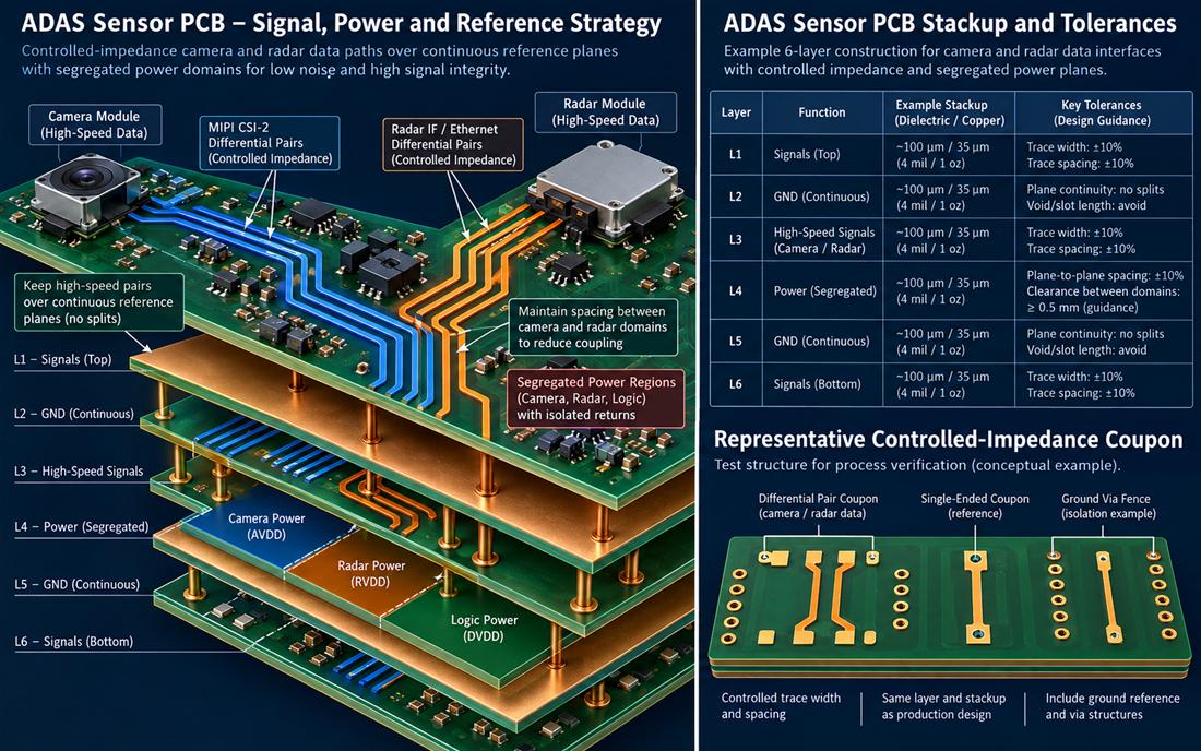
Start with the product budget: operating bands, bus speed, route length, connector count, allowable timing or phase margin, power-current density, and the enclosure reference. Map each requirement to a board variable. Dielectric height controls field confinement; copper roughness contributes conductor loss; plane continuity controls return inductance; and copper distribution affects press flow and warp. A ADAS Sensor PCB review should show which layers are functional RF or high-speed layers and which are only mechanical or power layers.
The program file should cross-reference via design and surface finish PCB so design and sourcing see the same boundary. The released ADAS Sensor PCB page is an internal capability reference; the engineering decision remains in this article and the project file.
Select material by tolerance and field behavior
Do not choose a laminate by brand name alone. Record resin content, pressed thickness, copper foil, glass style or glass-free construction, moisture assumption, and the tolerance used for the impedance model. Rogers’ automotive material literature shows why a cap-layer material can be combined with FR-4 for a 76–81 GHz board, while Analog Devices emphasizes that layout and manufacturing rules must be reviewed together. On the shop floor, the PCB materials drawing and the high frequency PCB design file must reference the same construction revision.
The handoff should name turnkey PCB assembly, PCB materials, and high frequency PCB design where those terms describe a controlled physical feature. The released ADAS Sensor PCB page is an internal capability reference; the engineering decision remains in this article and the project file.
Protect every return-current transition
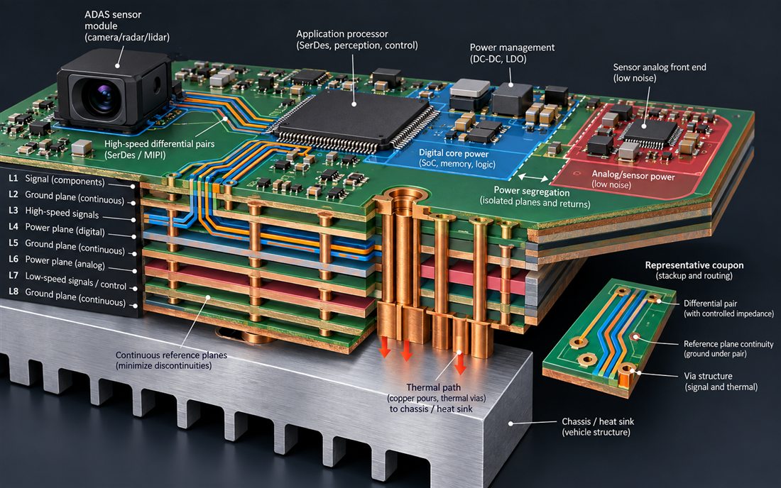
Treat the return path as a layer in its own right. A split plane, connector antipad, thermal clearance, or shield opening can force current around a longer loop. For ADAS Sensor PCB, walk every layer change in a 3-D view and mark the nearest return vias or bridge capacitors. Keep high-speed pairs away from plane edges and provide a defined path under the connector, sensor aperture, and power transition. A visually balanced stackup can still be electrically discontinuous if the return path is omitted from the drawing. Keep controlled impedance PCB beside the drawing revision and assign PCB manufacturing as the verification owner.
The released ADAS Sensor PCB page is an internal capability reference; the engineering decision remains in this article and the project file.
Build a tolerance stack, not a nominal picture
Build a tolerance stack that includes pressed dielectric, copper thickness, etch bias, registration, plated-hole position, solder-mask opening, and the mechanical datum used by the housing. Define which value is a design target and which value will be checked on a coupon or cross-section. If a prototype uses a broader engineering range, do not let that range silently become the production acceptance band. A project manager should be able to see the cost and schedule impact of tightening each variable before the design is frozen. The traveller can connect PCB assembly with automotive PCB design and preserve evidence for the next lot.
The released ADAS Sensor PCB page is an internal capability reference; the engineering decision remains in this article and the project file.
Release the construction with evidence
Release the construction with a representative coupon, measurement method, fixture, acceptance band, and change owner. The PCB manufacturing traveller should name the same laminate, copper, drill, and press revision used in the simulation or impedance calculation. A material substitution or press-cycle change is a new engineering decision, not an administrative update. Before sign-off, confirm signal integrity and DFM review use the same revision and acceptance method.
Release checklist for the next vehicle build
- State the vehicle interface, operating band, and environmental boundary for ADAS Sensor PCB.
- Identify the controlled material construction, copper profile, and pressed dielectric tolerance.
- Show the signal and return path through connectors, vias, shields, planes, and housing datums.
- Tie fabrication and assembly checks to a revisioned drawing, coupon, or inspection record.
- Label typical values, design targets, engineering ranges, and measured values separately.
- Record the owner and closure evidence for each open RF, thermal, mechanical, and service risk.
Sources: Analog Devices mixed-signal layout guidance; Rogers autonomous-driving material notes; Qorvo sensor front-end documents; and Würth high-speed interconnect application notes. These authoritative engineering references inform the reasoning; no external link is inserted into the article and no customer measurement, certification, or simulation result is implied without retained project evidence.
